Photodetector in germanium on silicon

a technology of germanium and silicon, applied in the field of photodetectors, can solve the problem of relative small thickness of the active layer, and achieve the effect of reducing metal losses

Active Publication Date: 2012-04-03
GOOGLE LLC
View PDF22 Cites 31 Cited by
  • Summary
  • Abstract
  • Description
  • Claims
  • Application Information

AI Technical Summary

Benefits of technology

[0023]In this way, the light is absorbed into the thin sensitive layer of the poly-Ge / Si heterojunction in a distributed way, during propagation. This releases the strong constraint of device thickness being larger than 1 / α, (where α is the absorption coefficient) in order to maximize absorption efficiency.
[0027]The electron-hole pairs generated due to the absorption of light can be efficiently collected using suitable metal contact structures fabricated according to the teaching of the invention.
[0030]The width W of the poly-Ge layer is preferably kept relatively low and in general minimized in order to limit the number of propagation modes and to maximize light intensity. However, calculation shows that losses due to the metallic contacts of the cathode (metal contact over the silicon waveguide) cannot be neglected for W<10 μm. The width W therefore is preferably larger than 10 μm and it depends on the shape of the contacts themselves.
[0033]According to a first preferred embodiment, the first contact covers completely the poly-Ge mesa, i.e. it has a length L and a width W. Being the first metal contact relatively wide, metallic losses can be relevant. Preferably, according to the first embodiment, the thickness T of the poly-Ge layer is comprised within 100 nm≦T≦160 nm in order to reduce the losses in the photodetector. Additionally, the preferred width W of the poly-Ge according to the first preferred embodiment is 10 μm≦W≦50 μm.
[0038]Due to the reduction of the metal losses in the second embodiment, the above mentioned constraints in terms of the upper and lower limit for T′ can be largely softened and the thickness T′ of the poly-Ge layer in this second embodiment can be selected within a wider range of values than in the first embodiment, preferably 60 nm≦T′≦200 nm and more preferably 80 nm≦T′≦180 nm.

Problems solved by technology

Applicants have noted that one of the main drawbacks of poly-Ge photodetectors in normal incidence detection is the relatively small thickness of the active layer of the poly-Ge heterojunction, e.g., about 50 nm for thermally evaporated poly-Ge.

Method used


Image

  • Photodetector in germanium on silicon
  • Photodetector in germanium on silicon
  • Photodetector in germanium on silicon

Examples


example 1

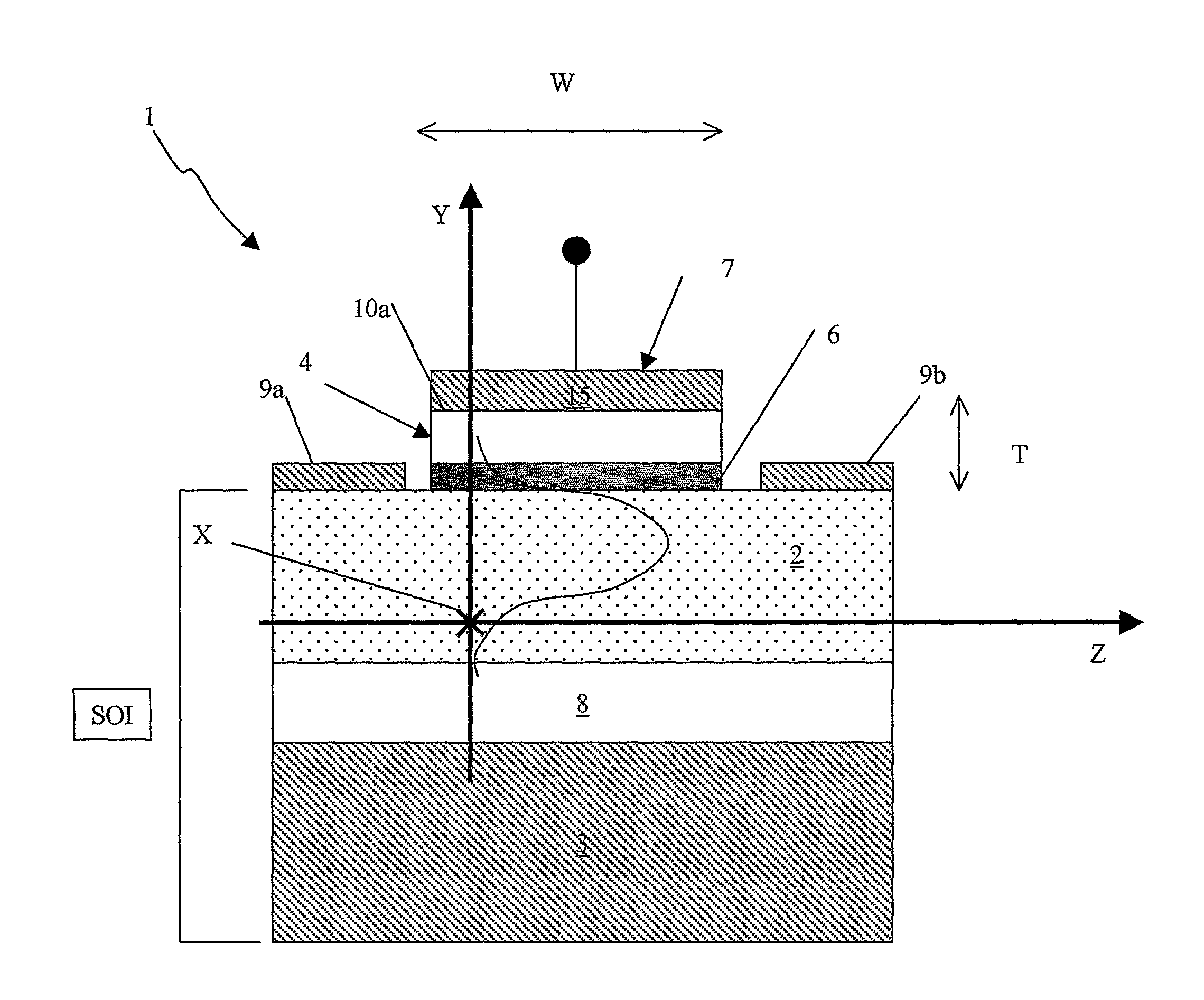
[0089]A Bond and Etch-back SOI substrate with 2 μm-thick n-type Si overlayer (2-3 Ωcm) and 1.5 μm-thick SiO2 insulator has been used. The samples were cleaved, but the input facets were un-polished.

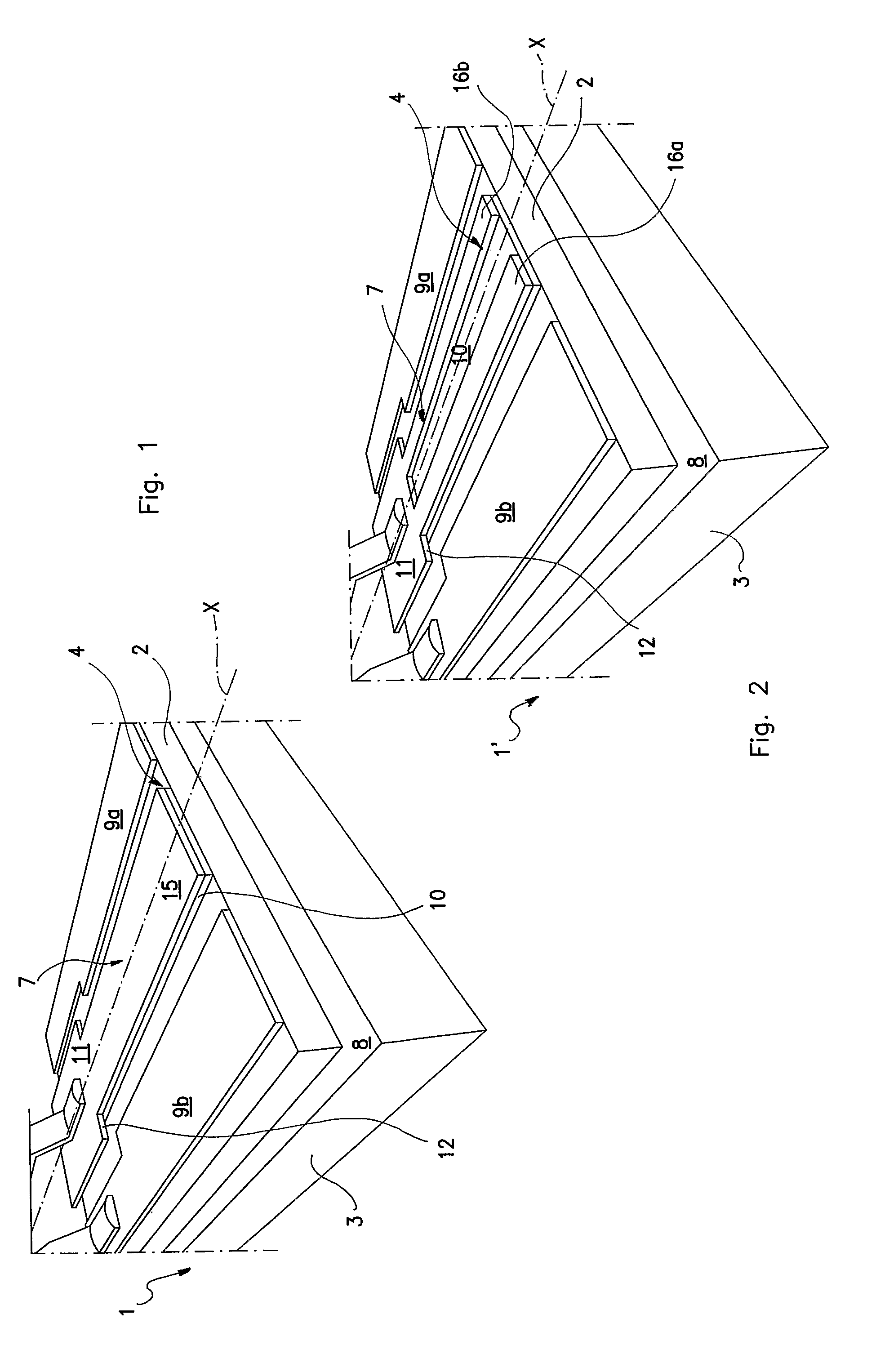
[0090]Polycrystalline Ge film was grown by thermal evaporation using a 99.999%-purity commercial source and a tungsten crucible in vacuum with a background pressure of 10−6-10−7 Torr. The substrate was heated by a massive copper-plate, temperature-stabilized at 300° C. by a thermo-coaxial cable. The Ge film thickness T was selected equal to 120 nm. Before the introduction into the vacuum chamber, the SOI substrate was chemically cleaned at room temperature by dipping them into buffered hydrofluoric acid (BHF) for 10 s. Poly-Ge mesa 10 was defined by lithography and selective wet-etching.

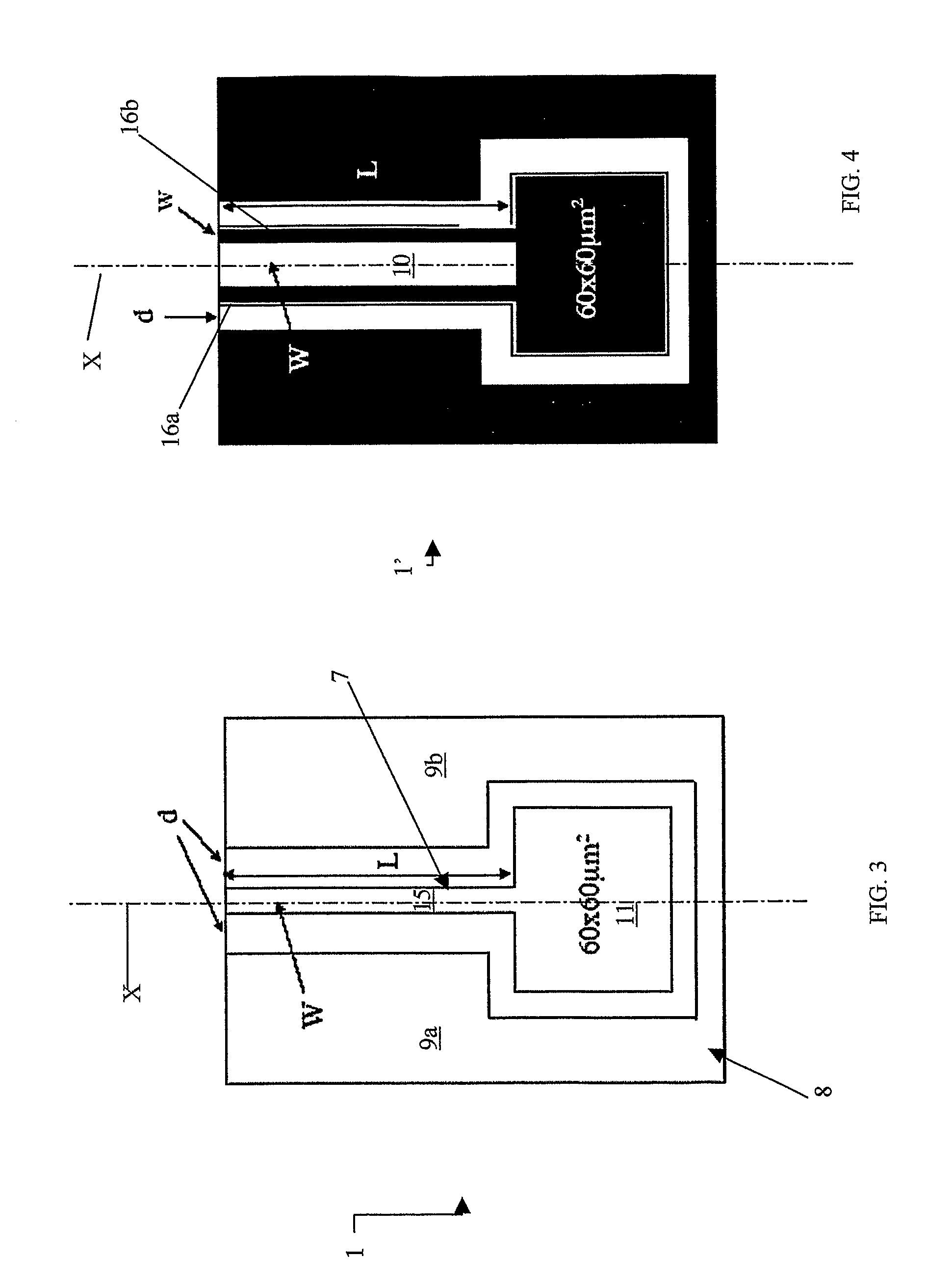
[0091]Aluminum contacts were subsequently deposited by thermal evaporation and defined by standard lithography. The square pad for wire bonding is of about 60×60 μm2.

[0092]Several devices has been fabricat...


PUM


Abstract

A photodetector structure includes a silicon-based waveguide in which optical signals to be detected travel in a given direction and are confined therein and a germanium layer disposed in contact with a portion of the silicon-based waveguide so that an evanescent tail of the propagating optical signal in the waveguide is coupled into the germanium layer. In addition, the germanium layer includes a mesa having a length along the signal propagating direction and a width in a direction substantially perpendicular to the propagating direction, in which the width of said mesa is smaller than its length. The photodetector also comprises a first and a second metal contacts, the first metallic contact being located on the germanium layer, the said second metallic contact being located on the silicon-based waveguide, the first and second contacts being used to collect electrons generated by light absorption to obtain an output electric signal.

Description

CROSS REFERENCE TO RELATED APPLICATION[0001]This application is a national phase application based on PCT / EP2004 / 014714, filed Dec. 24, 2004, the content of which is incorporated herein by reference.TECHNICAL FIELD[0002]The present invention relates to a photodetector realized in germanium on silicon, particularly a photodetector for near-infrared application. The selected geometries of the photodetector allow to achieve a good responsivity and excellent speed of the overall device.TECHNOLOGICAL BACKGROUND[0003]The introduction of fiber-based optical communication has brought a great increase of long haul telecommunications: the inherent low cost, wide bandwidth and small attenuation of fibers are key factors in prevailing over copper wire. In short haul access network, however, fiber qualities are superseded by the current high costs of optical transceivers. These components are usually hybrid assembly of III-V devices such as lasers, modulators, photodiodes and waveguide.[0004]In ...

Claims


Application Information

Patent Timeline
Patent Type & Authority Patents(United States)
IPC IPC(8): H01L31/0232
CPCH01L31/109H01L31/1808G02B6/4204Y02E10/50
Inventor MASINI, GIANLORENZOCOLACE, LORENZOASSANTO, GAETANO
Owner GOOGLE LLC
Why Eureka
Try Eureka