Dll circuit and semiconductor device having the same

a technology of dll circuit and semiconductor device, applied in the direction of digital storage, pulse automatic control, instruments, etc., can solve the problems of increasing reducing the size of the effective window used for capturing input/output data, etc., to reduce the possibility of data latching failure, reduce the time difference due to jitter appearing on the interpolated signal, and improve reliability

Inactive Publication Date: 2007-09-13
LONGITUDE SEMICON S A R L
View PDF19 Cites 18 Cited by
  • Summary
  • Abstract
  • Description
  • Claims
  • Application Information

AI Technical Summary

Benefits of technology

[0019]As descried above, according to the invention, when performing phase control using a reference clock signal, two delayed signals having delay times different by one cycle are interpolated. And when the reference clock signal including jitter at a certain cycle is input, the jitter appears at different cycles for the two delayed clock signals. Thus, timing difference due to jitter appearing on the interpolated signal can be reduced to half compared to the original reference clock signal. Accordingly, in a predetermined signal to be output, a reduced amount of an effective window corresponding to occurrence of jitter is also reduced to half, so that possibility of data latching failure is reduced and reliability can be improved.

Problems solved by technology

Therefore, it is a problem that size of an effective window used for capturing input / output data is reduced by an amount of the time Δ, and correspondingly, the possibility of data latching failure increases.

Method used


Image

  • Dll circuit and semiconductor device having the same
  • Dll circuit and semiconductor device having the same
  • Dll circuit and semiconductor device having the same

Examples


Embodiment Construction

[0032]A preferred embodiment of the invention will be described below with reference to accompanying drawings. In this embodiment, a semiconductor device to which the present invention is applied is, for example, a DDR-SDRAM as a synchronous type semiconductor device having a DLL circuit for generating DQS and DQ signals. The configuration and operation of this embodiment will be described below using FIGS. 1 to 7.

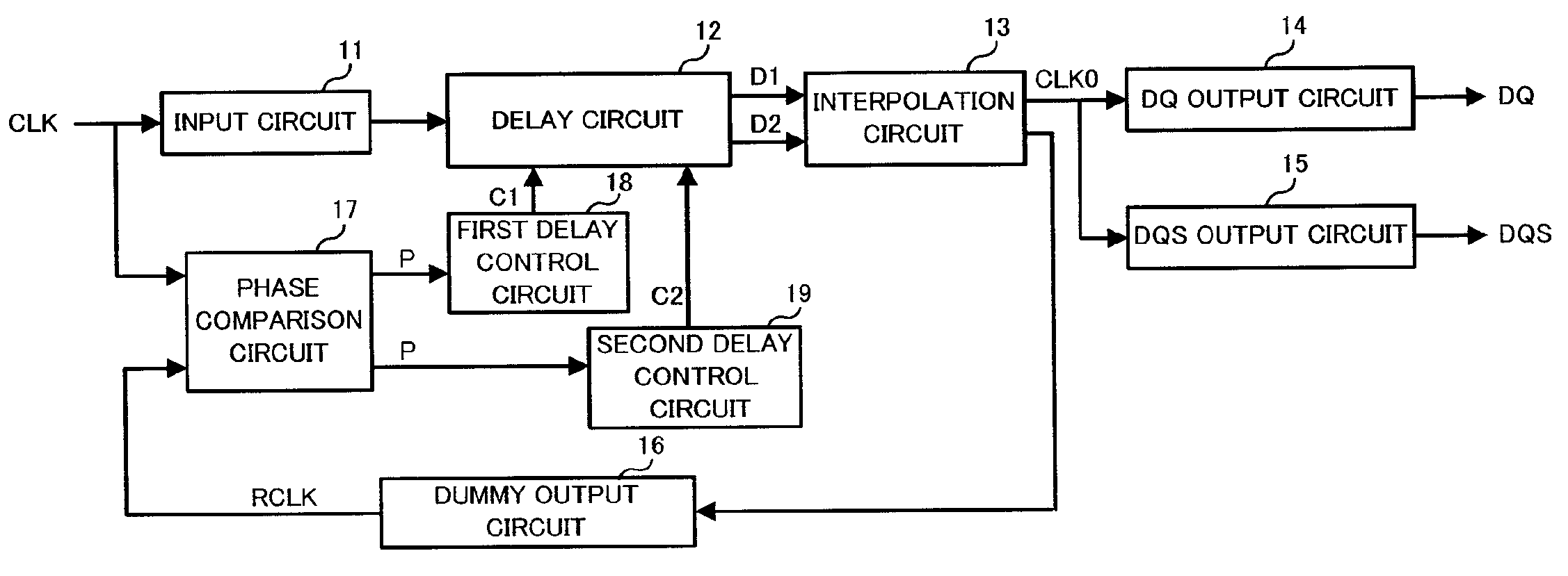
[0033]FIG. 1 is a block diagram showing a configuration of a DLL circuit of this embodiment. The DLL circuit shown in FIG. 1 includes an input circuit 11, a delay circuit 12, an interpolation circuit 13, a DQ output circuit 14, a DQS output circuit 15, a dummy output circuit 16, a phase comparison circuit 17, a first delay control circuit 18 and a second delay control circuit 19, and has a function of generating DQ and DQS signals required for data input / output in the DDR-SDRAM.

[0034]In the above configuration, a reference clock signal CLK from the outside is buffered by t...


PUM


Abstract

A DLL circuit comprising: delay circuits which output first and second delayed clock signals obtained by delaying the reference clock signal by a delay times selected according to control signals; an interpolation circuit which interpolates a phase difference between the delayed clock signals to output an internal clock signal; an output circuit which generates a predetermined signal; a dummy output circuit which has the same transmission characteristics as the output circuit and outputs a feedback clock signal having the same phase as the predetermined signal; a phase comparison circuit which compares phases of the reference clock signal and the feedback clock signal; delay control circuits which controls the control signals in a direction where both phases are equal; wherein the delay time of the second delayed clock signal is larger than the first delayed clock signal by an amount equivalent to one cycle of the reference clock signal.

Description

BACKGROUND OF THE INVENTION[0001]1. Field of the Invention[0002]This invention relates to a DLL (Delay Locked Loop) circuit, and particularly relates to a DLL circuit which generates an internal signal having a predetermined time difference relative to an external clock signal and a semiconductor device (for example, a synchronous type semiconductor device) having this DLL circuit.[0003]2. Related Art[0004]Recently, DDR-SDRAM (Double Data Rate—Synchronous Dynamic Random Access Memory) is widely known as a high speed synchronous type semiconductor memory device. When read operation is performed in the DDR-SDRAM, each edge timing of a DQ signal being input / output data and a DQS signal for determining a timing to capture input / output data needs to be controlled to have an accurate phase relationship with an external reference clock. Therefore, a DLL circuit for generating the DQS and DQ signals by phase control based on the reference clock signal (for example, see JP-2003-91331).[0005]...

Claims


Application Information

Patent Timeline
Patent Type & Authority Applications(United States)
IPC IPC(8): H03L7/06G11C11/407G11C11/4076H03K5/13H03K5/131H03L7/081
CPCH03L7/107H03L7/0814H03L7/0816
Inventor TAKAI, YASUHIRO
Owner LONGITUDE SEMICON S A R L
Why Eureka
Try Eureka