Anodized metal substrate module

Active Publication Date: 2007-09-20
SAMSUNG ELECTRONICS CO LTD
View PDF10 Cites 69 Cited by
  • Summary
  • Abstract
  • Description
  • Claims
  • Application Information

AI Technical Summary

Benefits of technology

[0008]The present invention has been made to solve the foregoing problems of the prior art and therefore an aspect of the present invention is to provide an anodized metal substrate mod

Problems solved by technology

However, a typical PCB, if mounted with a device such as a light emitting diode or a power chip which generates a considerable amount of heat, is degraded in reliability due to poor heat transfer properties thereof.
The typical PCB with inferior heat radiation properties proves disadvantageous for a backlight unit of

Method used


Image

  • Anodized metal substrate module
  • Anodized metal substrate module
  • Anodized metal substrate module

Examples


example

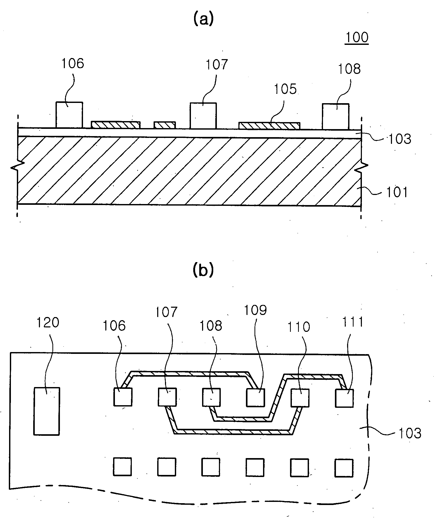
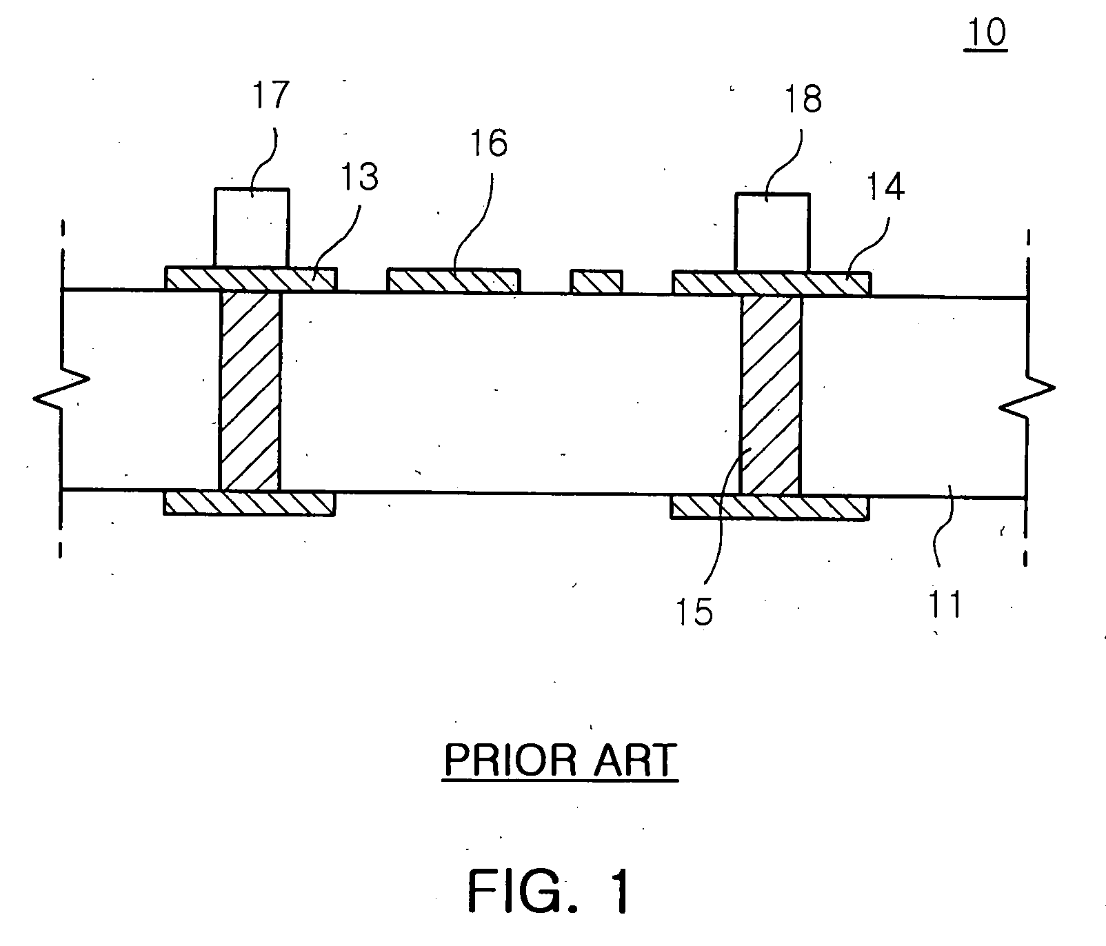
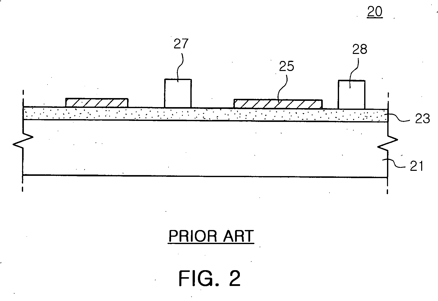
[0047]To compare and confirm heat transfer properties between a PCB or MCPCB and an anodized metal substrate module of the invention, the inventors conducted tests based on computer simulation. For these simulation tests, samples were set according to comparative example 1, comparative example 2, and inventive example. Comparative example 1 was a conventional resin (FR4)-based PCB configured as in FIG. 1. Comparative example 2 was an MCPCB using an Al core (refer to FIG. 2). The inventive example, as shown in FIG. 3, was an anodized substrate module with a stacked structure of an ‘Al plate / an Al anodized film.’ In comparative example 2, the MCPCB included a conventional polymer insulating layer having a heat conductive coefficient of about 1.3 W / mK. In contrast, the Al anodized film had a heat transfer coefficient of 10 W / mK to 30 W / mK.

[0048]FIGS. 9 to 11 illustrate simulation results for heat resistance regarding the three samples (comparative example 1, comparative example 2 and i...


PUM


Abstract

An anodized metal substrate module superior in heat radiation properties and reduced in manufacturing costs. A metal plate is provided. An anodized film is formed on the metal plate. A heat generating device is mounted on the metal plate. Also, a conductive line is formed on the anodized film.

Description

CLAIM OF PRIORITY[0001]This application claims the benefit of Korean Patent Application No. 2006-25010 filed on Mar. 17, 2006 in the Korean Intellectual Property Office, the disclosure of which is incorporated herein by reference.BACKGROUND OF THE INVENTION[0002]1. Field of the Invention[0003]The present invention relates to a substrate module mounted with a heat generating device such as a light emitting diode and a power chip, and more particularly, to an anodized metal substrate module superior in heat radiation properties, which can be applied to a backlight unit and a surface light source device.[0004]2. Description of the Related Art[0005]Recently, researches have been under way to improve heat radiation properties of a circuit board. Conventionally, a heat generating device has been mounted on a printed circuit board (PCB) having an insulating base substrate. However, a typical PCB, if mounted with a device such as a light emitting diode or a power chip which generates a cons...

Claims


Application Information

Patent Timeline
IPC IPC(8): F21V7/04
CPCF21K9/00H05K1/021H05K1/053H05K1/182H05K2201/0347F21V29/89H05K2203/0315H01L2924/0002H05K2201/10106F21V29/76H01L2924/00G02B6/0053G02B6/0061G02B6/0068G02B6/0073
Inventor LEE, YOUNG KICHOI, SEOG MOONYOON, YOUNG BOKSHIN, SANG HYUN
Owner SAMSUNG ELECTRONICS CO LTD
Why Eureka
Try Eureka