

Method of fabricating nitride-based semiconductor light-emitting device and nitride-based semiconductor light-emitting device
a technology of nitride-based semiconductors and light-emitting devices, which is applied in the direction of semiconductor devices, semiconductor lasers, semiconductor lasers, etc., can solve the problems of large number of cracks formed on n-type algan layers, large number of cracks formed, and large number of disadvantageous cracks, so as to achieve the effect of reducing the luminous efficiency, and improving the luminous efficiency
- Summary
- Abstract
- Description
- Claims
- Application Information
AI Technical Summary
Benefits of technology
Problems solved by technology
Method used
Image

Examples
first embodiment
[0071]A method of fabricating a nitride-based semiconductor laser diode according to a first embodiment of the present invention is described with reference to FIGS. 1 to 12 and 34.
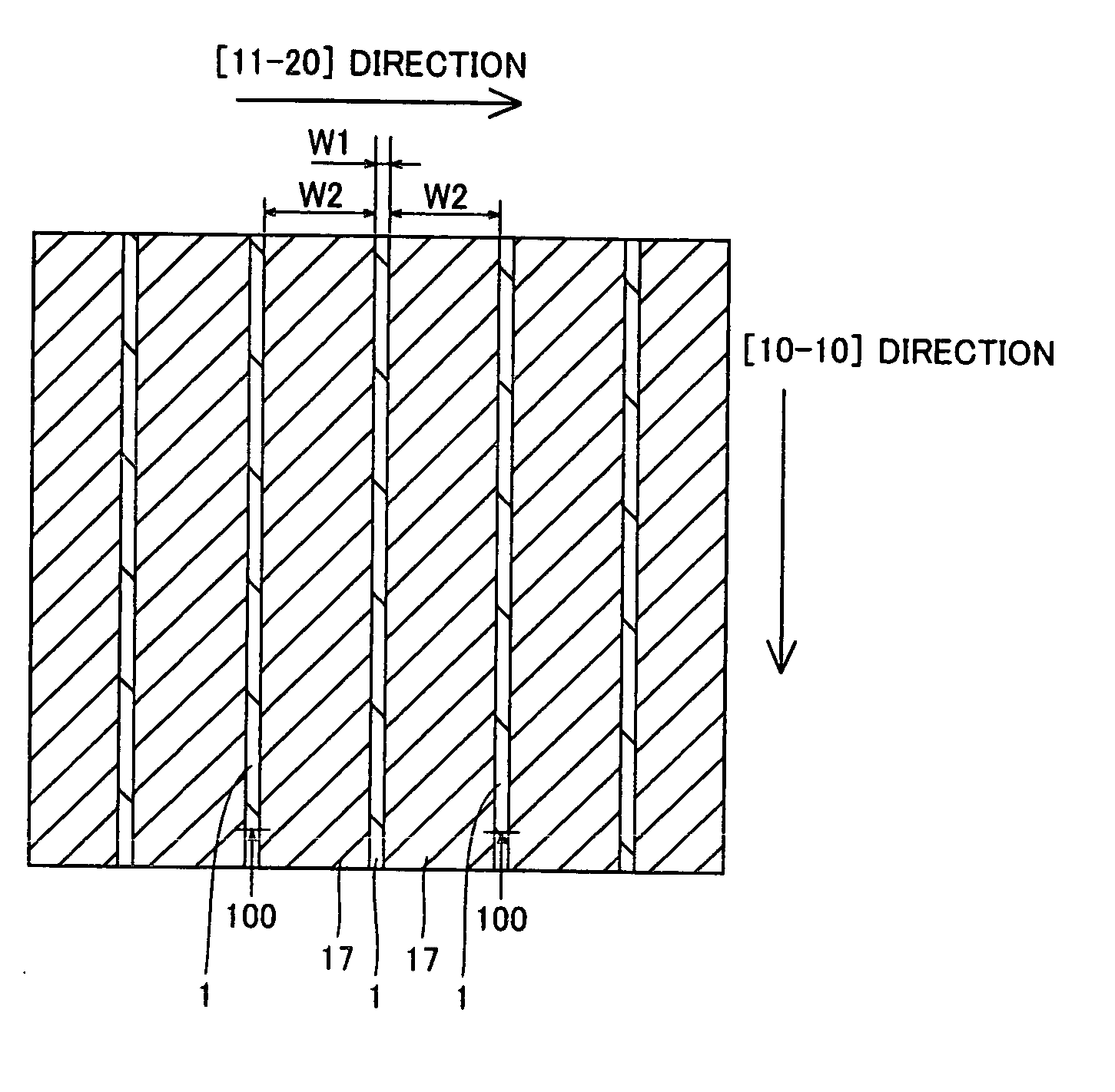
[0072]In the method of fabricating a nitride-based semiconductor laser diode according to the first embodiment, an n-type GaN substrate 1 having a surface of the (0001) plane with a low dislocation density is prepared, as shown in FIGS. 1 and 2. This n-type GaN substrate 1 has a lattice constant of about 0.3189 nm (a-axis direction). The n-type GaN substrate 1 is an example of the “nitride-based semiconductor substrate” in the present invention. Then, striped (slender) mask layers 17 of Ni each having a thickness of about 0.4 μm are formed on prescribed regions of the n-type GaN substrate 1 by electron beam evaporation or the like. More specifically, the mask layers 17 are so formed as to extend in the [1-100] direction. Further, the distance W1 between the mask layers 17 adjacent to each other along the ...
second embodiment
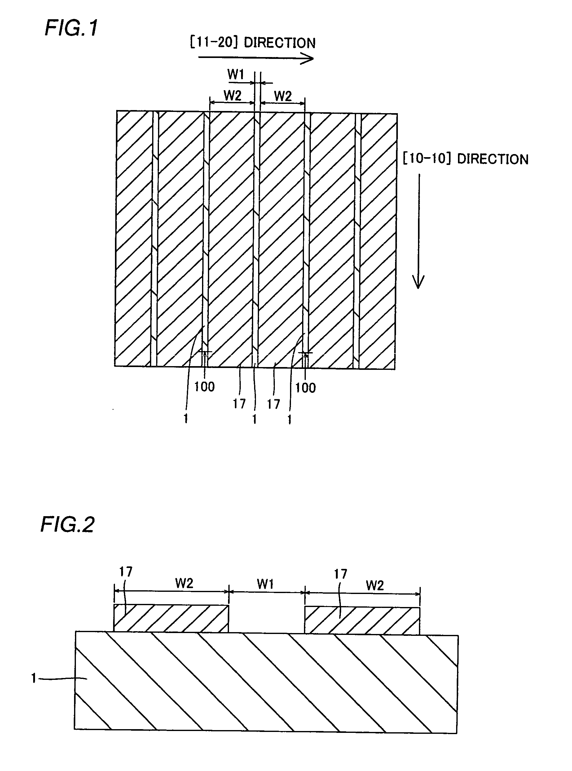
[0091]Referring to FIGS. 13 to 15 and 34, striped (slender) groove portions 21a extending in the [11-20] direction are formed on an n-type GaN substrate 21 in a method of fabricating a nitride-based semiconductor laser diode according to a second embodiment of the present invention, dissimilarly to the aforementioned first embodiment.
[0092]In the method of fabricating a nitride-based semiconductor laser diode according to the second embodiment, the striped (slender) groove portions 21a each having a width W11 of about 50 μm and a depth of about 2 μm with side surfaces perpendicular to the upper surface of the n-type GaN substrate 21 are formed on the n-type GaN substrate 21 through steps similar to those in the first embodiment shown in FIGS. 1 to 4, as shown in FIG. 13. According to the second embodiment, however, the groove portions 21a are so formed as to extend in the [11-20] direction. The distance W12 between the groove portions 21a adjacent to each other along the [1-100] dir...
third embodiment
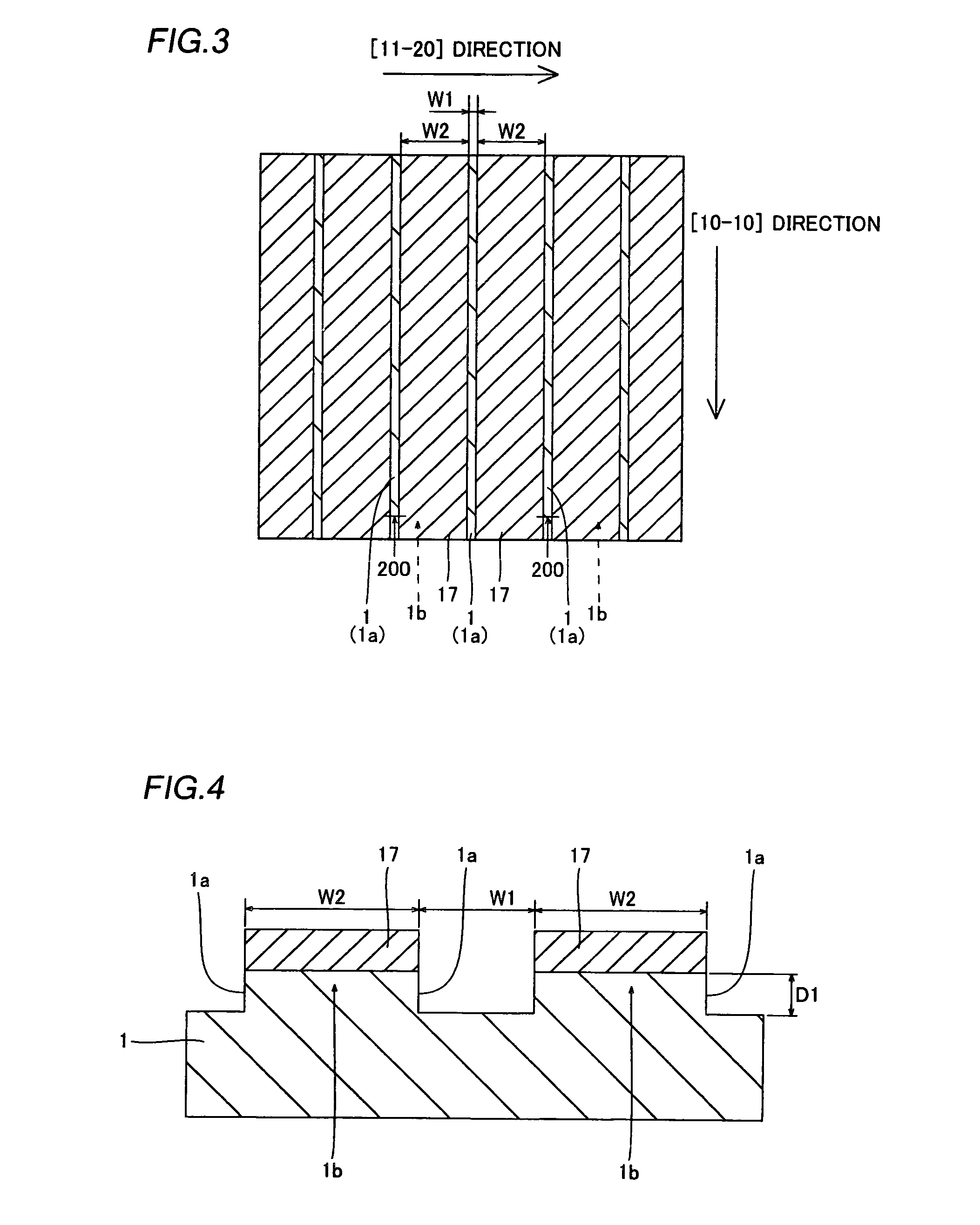
[0103]Referring to FIGS. 16 and 34, striped (slender) groove portions 41a and 41b extending in the [1-100] direction and the [11-20] direction respectively are latticed on an n-type GaN substrate 41 in a method of fabricating a nitride-based semiconductor laser diode according to a third embodiment of the present invention, dissimilarly to the aforementioned first and second embodiments.
[0104]In the method of fabricating a nitride-based semiconductor laser diode according to the third embodiment, the striped (slender) groove portions 41a and 41b each having a width W21 of about 50 μm and a depth of about 2 μm with side surfaces perpendicular to the upper surface of the n-type GaN substrate 41 are formed on the n-type GaN substrate 41 through steps similar to those of the first embodiment shown in FIGS. 1 to 4, as shown in FIG. 16. According to the third embodiment, however, the groove portions 41a and 41b are so latticed as to extend in the [1-100] direction and the [11-20] directio...
PUM
 Abstract
Description
Claims
Application Information