Semiconductor device with increased channel area and decreased leakage current

Inactive Publication Date: 2007-09-27
SK HYNIX INC
View PDF5 Cites 10 Cited by
  • Summary
  • Abstract
  • Description
  • Claims
  • Application Information

AI Technical Summary

Benefits of technology

[0012] The present invention relates to a semiconductor device and a method for fabricating the same wherein a recess channel region including vertical silicon-on-insulator (SOI) channel structures, which are disposed at sidewalls of both device isolation structures under a gate in a longitudinal direction of a gate region, is formed, thereby increasing a channel area of the device and decreasing its leakage current. Accordingly, the short channel effect (SCE) and refresh characteristics of the device can be improved.

Problems solved by technology

This results in degradation of the refresh characteristics of the dynamic random access memory (DRAM) structure.
According to the above conventional method for fabricating a semiconductor device, the device isolation structure of the gate region is etched to protrude the Fin-type active region, which necessarily causes loss of the protruded Fin-type active region during a subsequent cleaning process including hydrogen fluoride (HF).
Accordingly, it is difficult to pattern the gate structure due to its increased complexity.

Method used


Image

  • Semiconductor device with increased channel area and decreased leakage current
  • Semiconductor device with increased channel area and decreased leakage current
  • Semiconductor device with increased channel area and decreased leakage current

Examples


Embodiment Construction

[0021] The present invention relates to a semiconductor device and a method for fabricating the same wherein a recess channel region including vertical silicon-on-insulator (SOI) channel structures, which are disposed at sidewalls of both device isolation structures under a gate in a longitudinal direction of a gate region, is formed, thereby increasing a channel area of the device and decreasing its leakage current. Accordingly, the short channel effect (SCE) and refresh characteristic of the device can be improved.

[0022]FIG. 4 is a simplified layout of a semiconductor device according to an embodiment of the present invention, wherein reference numerals 101 and 103 denote an active region defined by the device isolation structure 130 and a gate region, respectively.

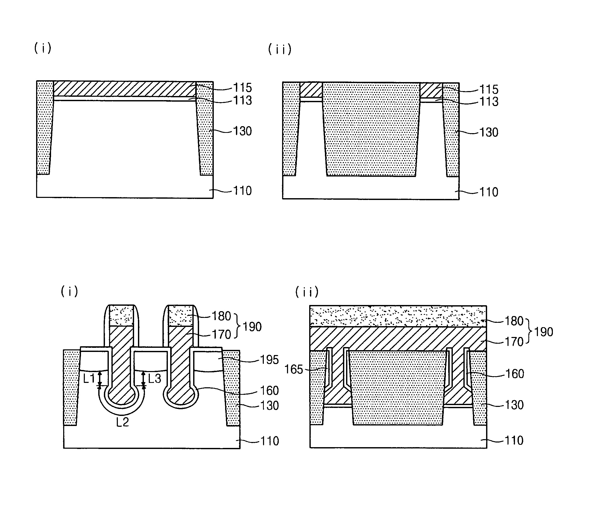
[0023] FIGS. 5(i) and 5(ii) are simplified cross-sectional views of a semiconductor device according to an embodiment of the present invention, wherein FIG. 5(i) is a cross-sectional view taken along a longitudinal di...


PUM


Abstract

The semiconductor device includes an active region, a recess channel region including vertical channel structures, a gate insulating film, and a gate structure. The active region is defined by a device isolation structure formed in a semiconductor substrate. The recess channel region is formed in the active region. The vertical silicon-on-insulator (SOI) channel structures are disposed at sidewalls of both device isolation structures in a longitudinal direction of a gate region. The gate insulating film is disposed over the active region including the recess channel region. The gate structure is disposed over the recess channel region of the gate region.

Description

CROSS-REFERENCES TO RELATED APPLICATIONS [0001] The present application claims priority to Korean patent application No. 10-2006-0026511, filed on Mar. 23, 2006, which is incorporated by reference in its entirety. BACKGROUND OF THE INVENTION [0002] The present invention relates to a memory device. More particularly, the present invention relates to a semiconductor device and a method for fabricating the same having a recess channel region including vertical silicon-on-insulator (SOI) channel structures. [0003] When a channel length of a cell transistor is decreased, the ion concentration of a cell channel region is generally increased in order to maintain the threshold voltage of the cell transistor. An electric field in source / drain regions of the cell transistor is enhanced to increase the leakage current. This results in degradation of the refresh characteristics of the dynamic random access memory (DRAM) structure. Therefore, there is a need for semiconductor devices in which th...

Claims


Application Information

Patent Timeline
IPC IPC(8): H01L27/12H01L27/01H01L31/0392
CPCH01L21/823481H01L21/823487H01L29/785H01L27/1203H01L21/84H01L21/18
Inventor CHUNG, SUNG WOONGLEE, SANG DON
Owner SK HYNIX INC
Why Eureka
Try Eureka