Semiconductor radiation source and light curing device

a radiation source and semiconductor technology, applied in the field of semiconductor radiation sources, can solve the problems of comparatively complex sealing, large thermal radiation emission of high-power chips, and considerably more complicated matter to focus, and achieve the effect of improving the radiation sour

Inactive Publication Date: 2007-10-04
IVOCLAR VIVADENT AG
View PDF14 Cites 55 Cited by
  • Summary
  • Abstract
  • Description
  • Claims
  • Application Information

AI Technical Summary

Benefits of technology

[0009]Therefore, the invention is based on the object of providing a semiconductor radiation source wherein the radiation source is improved as regards the ratio between the lig

Problems solved by technology

This seal is comparatively complex since it must typically also be taken into account that the liquid expands on account of heating.
The resultant problems are greater the greater the heat loss generated by the LED chips, while, on the other hand, high-power chips, in particular, emit a very large amount of thermal radiation.
Although this also makes it possible to provide a very high overall optical power, it is a considerably more complicated matter to focus the light beam, especially whe

Method used


Image

  • Semiconductor radiation source and light curing device
  • Semiconductor radiation source and light curing device
  • Semiconductor radiation source and light curing device

Examples


Embodiment Construction

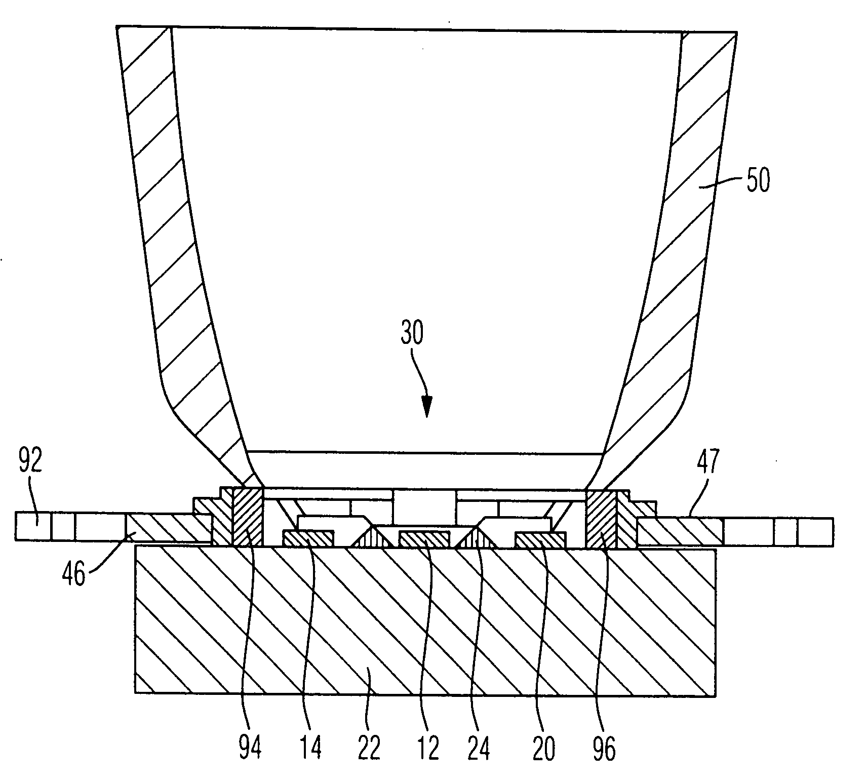
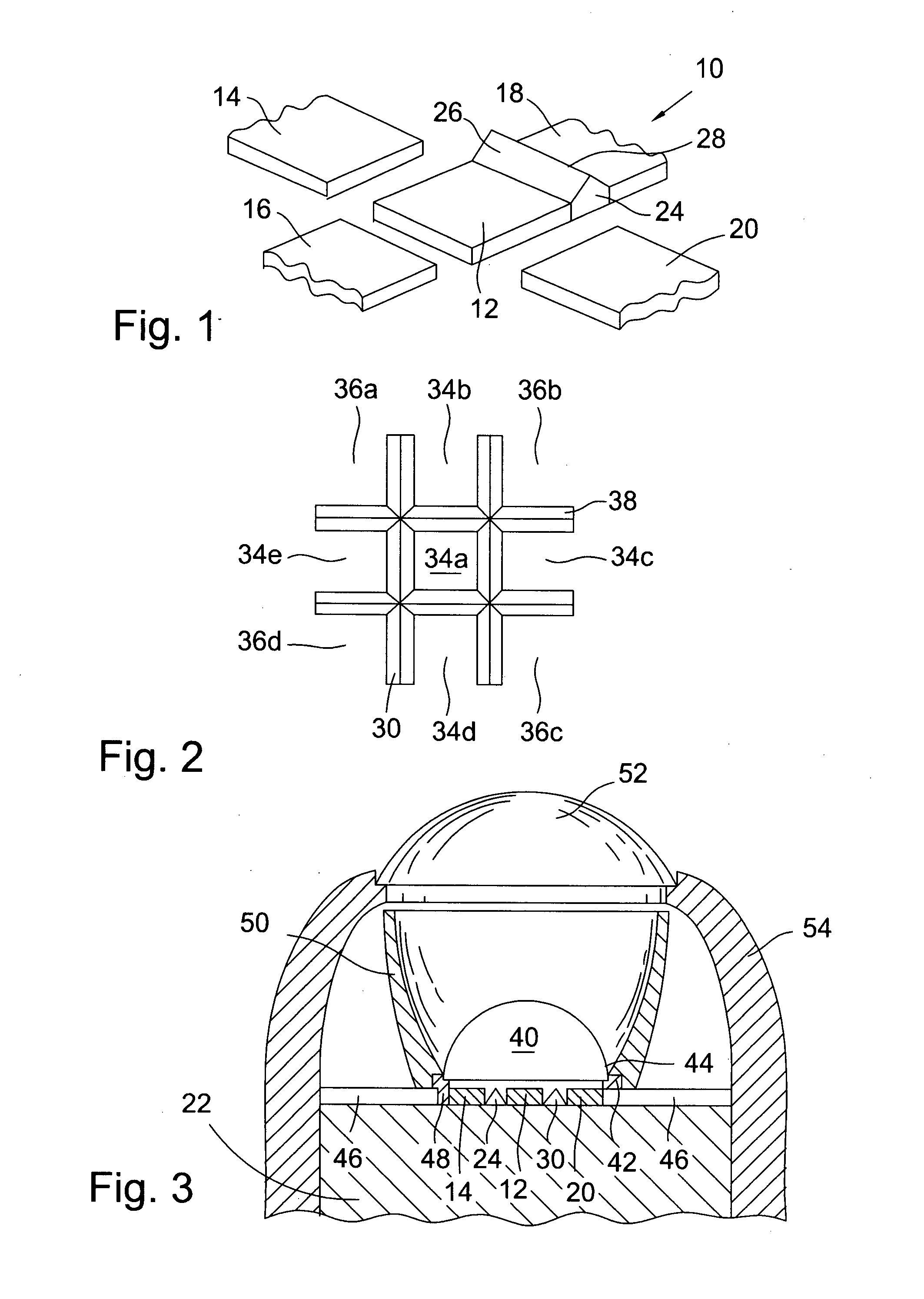
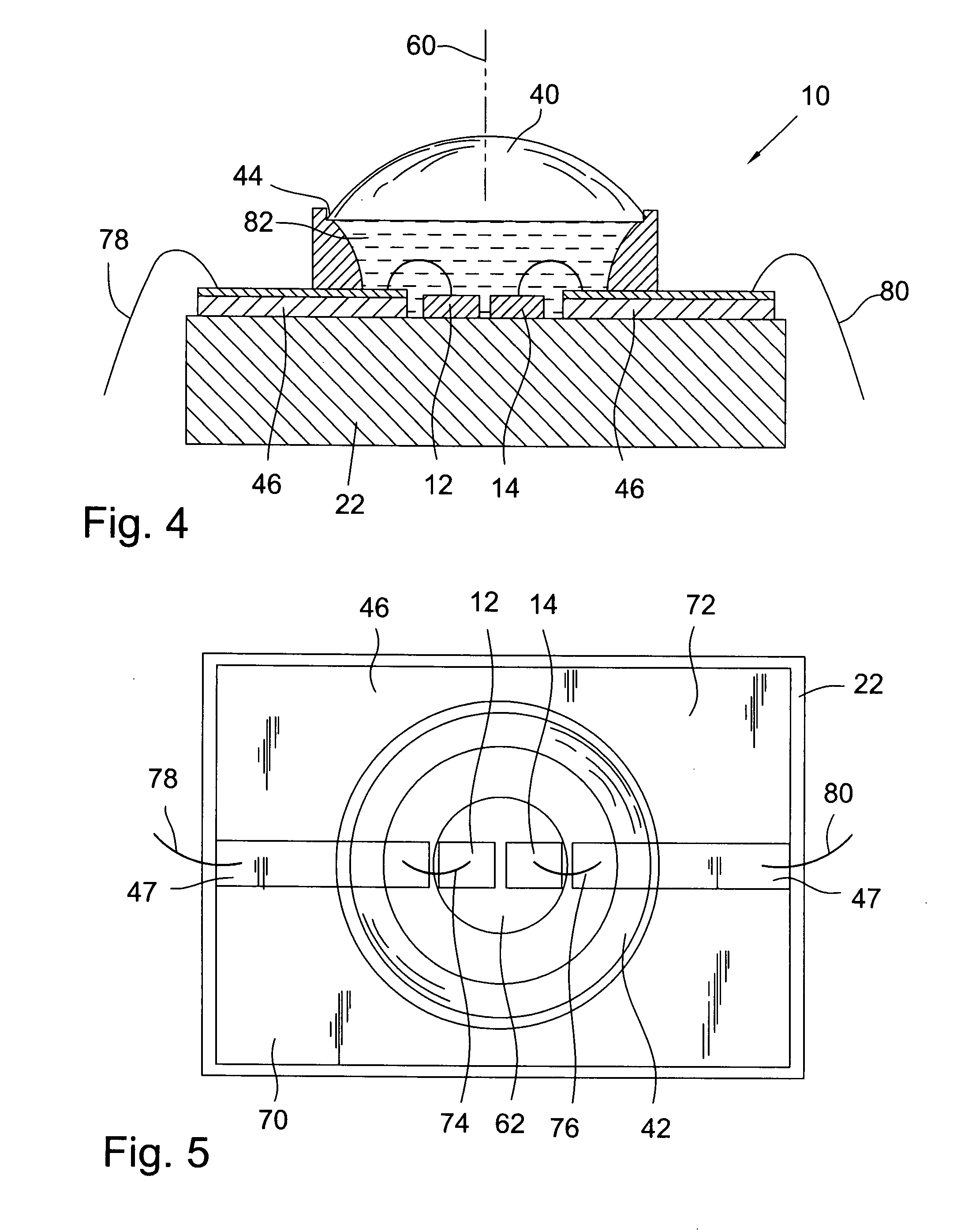
[0063]The semiconductor radiation source 10 which is partially illustrated in FIG. 1 has a plurality of LED chips (one centrally arranged chip 12 and four chips 14, 16, 18 and 20 which each extend along the side edges of said chip 12 in the exemplary embodiment illustrated). The chips are fitted to a base body 22 which is composed of metal and, at the same time, is used as a mounting base and as a heat sink. The base body is preferably at least partially composed of copper and / or is at least partially coated with gold or nickel / gold. Application is effected with a low thermal resistance between the chips and the base body 22, so that a high thermal power can also be dissipated.

[0064]A respective reflector element 24 which, in the side view, has an essentially roof-shaped structure is arranged between the central chip 12 and the adjacent chips 14 to 20. The reflector element 24 extends such that it adjoins the respective adjacent side areas of the LED chips 18 and 12 and is used to r...


PUM


Abstract

A semiconductor radiation source has a base body on which at least two LED chips are directly mounted and are fitted to the base body using a thermally conductive connection. At least one printed circuit board is mounted on the base body and extends from the centrally arranged LED chips to the outside, in particular to the peripheral region of the base body, and projects, in particular, into free areas which extend laterally beside the chips or between the latter.

Description

CROSS-REFERENCE TO RELATED APPLICATIONS[0001]This application claims foreign priority benefits under 35 U.S.C. §119 from German patent application Ser. No. 10 2006 015 377.4 filed Apr. 3, 2006.TECHNICAL FIELD[0002]The invention relates to a semiconductor radiation source having a base body, at least two centrally arranged LED chips directly mounted to the base body using a thermally conductive connection, and at least one printed circuit board mounted on the base body and which extends from the centrally arranged LED chips to the outside, in particular to the peripheral region of the base body.BACKGROUND OF THE INVENTION[0003]In the case of a semiconductor radiation source of this type, it has already been proposed to centrally mount at least two LED chips on a heat sink and to focus the light emitted by the LED chips using a common converging lens. The light emission is particularly efficient if the LED chips are arranged such that they are closely adjacent to the focal point of th...

Claims


Application Information

Patent Timeline
IPC IPC(8): H01L33/00F21K99/00H01L33/60H01L33/64
CPCA61C19/003H01L25/0753H01L33/60H01L33/64H01L33/648H01L2224/48091H01L2924/3025H01L2924/00014H01L2924/00
Inventor PLANK, WOLFGANGSENN, BRUNO
Owner IVOCLAR VIVADENT AG
Why Eureka
Try Eureka