Insulating substrate and semiconductor device

a technology of insulating substrate and semiconductor, which is applied in the direction of superimposed coating process, printed circuit aspects, coatings, etc., can solve the problems of high price, difficult application of insulating substrate, and high price of insulating substrate b>600/b> incorporating ceramic base substrate, etc., to achieve superior heat radiation and insulation performance, reduce the number of manufacturing steps, and reduce the effect of manufacturing steps

Active Publication Date: 2006-05-25
FUJI ELECTRIC HLDG CO LTD
View PDF4 Cites 59 Cited by
  • Summary
  • Abstract
  • Description
  • Claims
  • Application Information

AI Technical Summary

Benefits of technology

[0033] The invention as described above can provide an insulating substrate which is inexpensive because of a reduced number of manufacturing steps and is superior in heat radiation and insulation performance.

Problems solved by technology

However, it is difficult to apply the insulating substrate 500 to a power circuit module whose current capacity exceeds about 50 A.
However, there is a problem that the insulating substrate 600 incorporating the ceramic base substrate is expensive for the following reason.
As such, the insulating substrate 600 including ceramics as a material requires many manufacturing steps in forming the ceramic base substrate 601, resulting in a high price.

Method used


Image

  • Insulating substrate and semiconductor device
  • Insulating substrate and semiconductor device
  • Insulating substrate and semiconductor device

Examples


Embodiment Construction

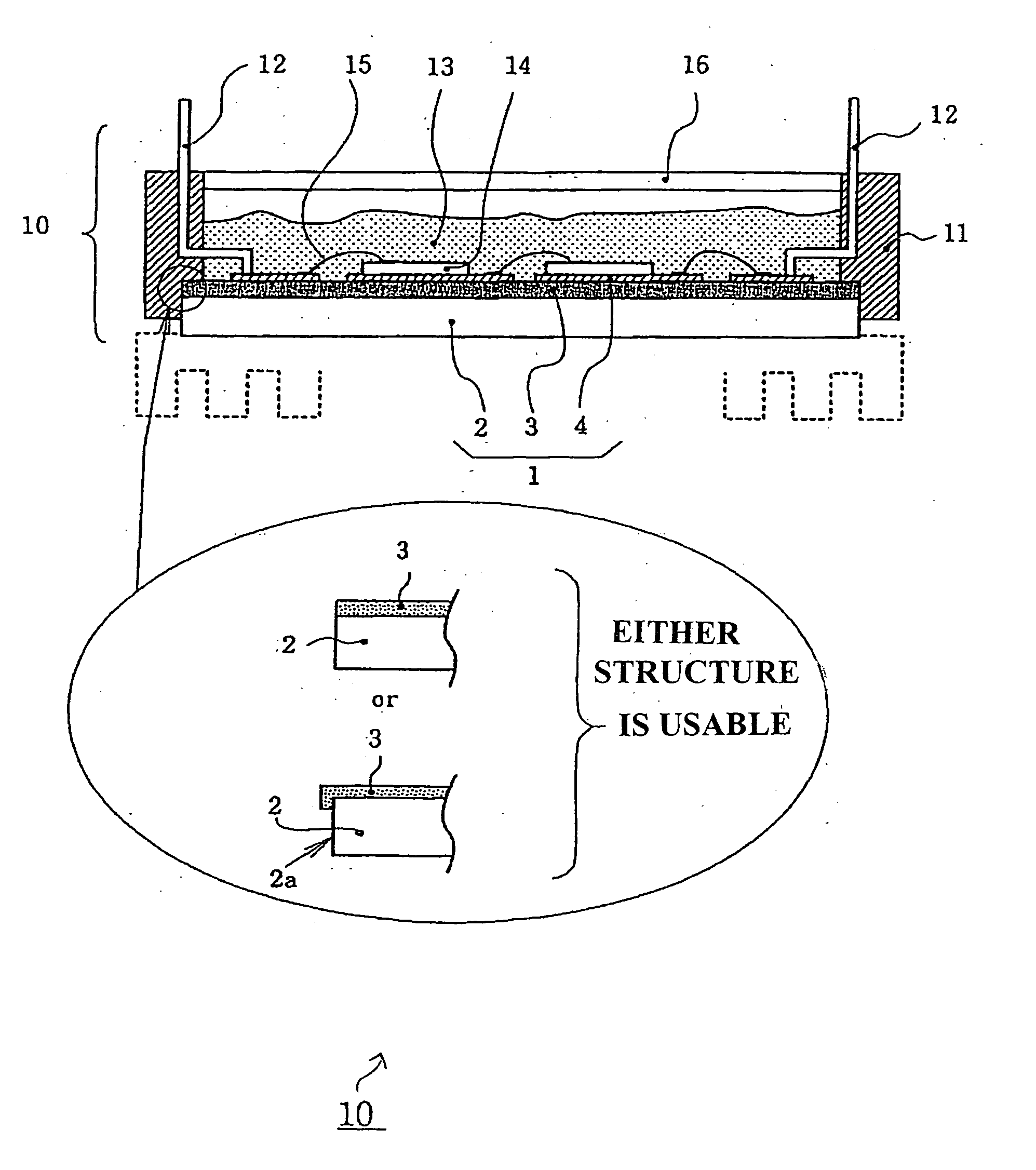
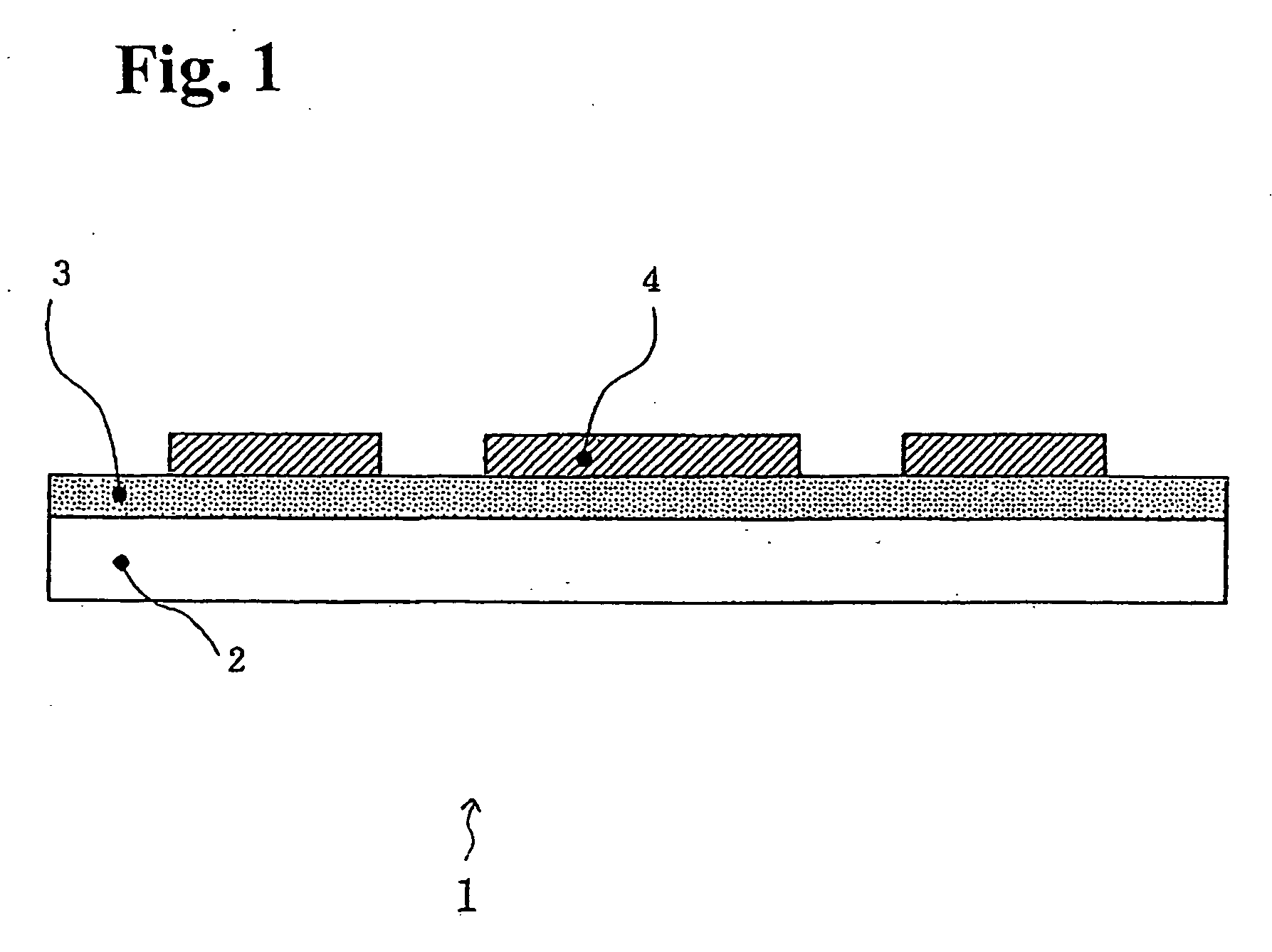
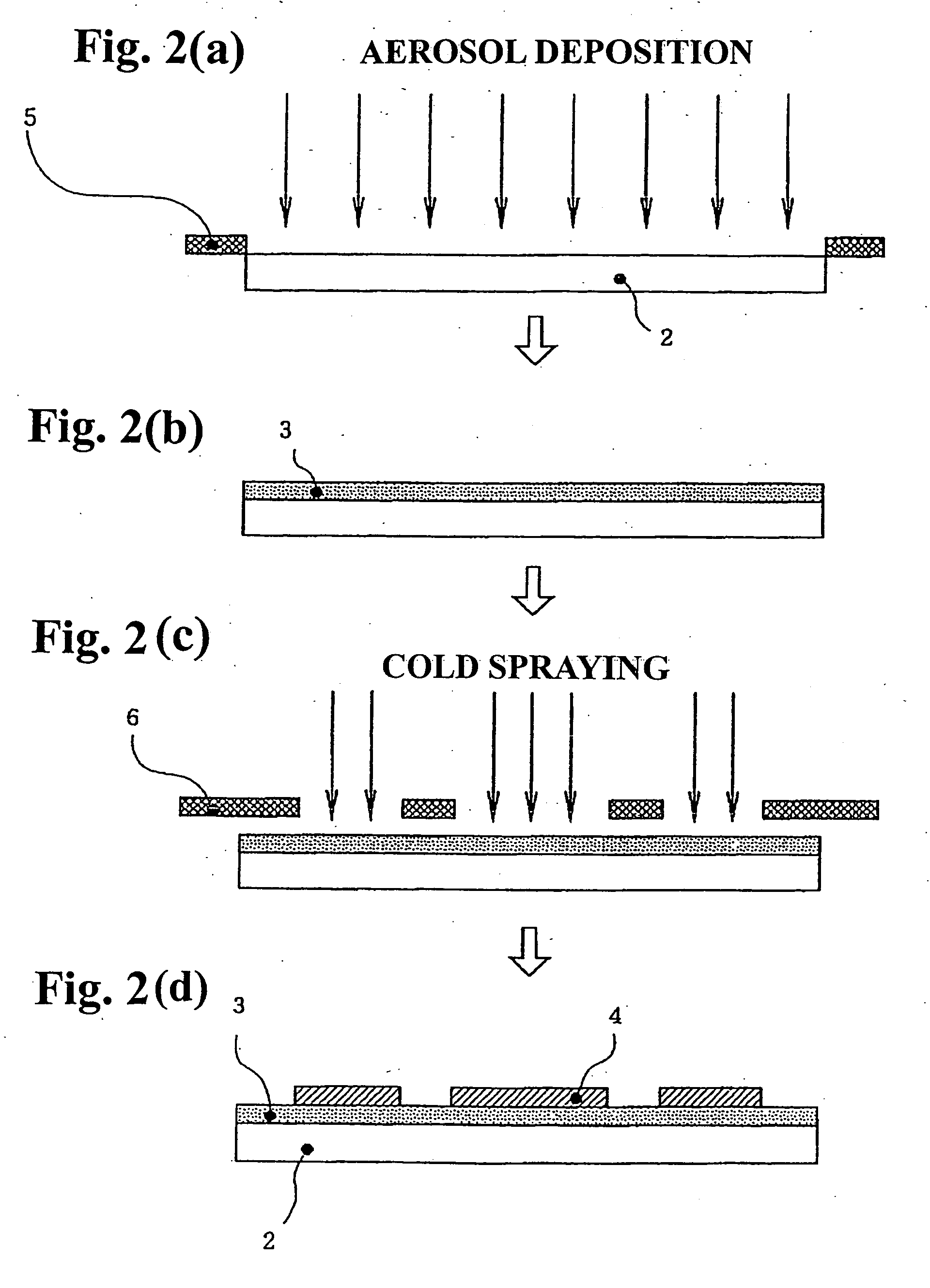
[0042] An insulating substrate and a semiconductor device according to embodiments of the present invention will be hereinafter described with reference to the drawings. FIG. 1 is a sectional view showing the structure of an insulating substrate according to one embodiment of the present invention. The insulating substrate 1 is provided with a metal base 2, an insulating layer 3, and a circuit pattern 4.

[0043] The metal base 2 is a metal plate such as an aluminum plate, an aluminum alloy plate, a copper plate, or a copper alloy plate.

[0044] The insulating layer 3 is a room temperature shock solidification film formed by an aerosol deposition method. The thickness of the insulating layer 3 is set taking the thermal resistance, the insulation characteristic, etc. into consideration, and is usually set at about 30-400 μm. Formed in a crystal state by the aerosol deposition method, the thermal conductivity of the insulating layer 3 becomes equal to or close to that of the bulk itself ...


PUM

PropertyMeasurementUnit
diameteraaaaaaaaaa
thicknessaaaaaaaaaa
current capacityaaaaaaaaaa

Abstract

An insulating substrate includes a metal base as a base member, an insulating layer which is a room temperature, aerosol deposited shock solidification film formed on the metal base, and a circuit pattern which is a cold sprayed thermal spray coating formed on the insulating layer. A semiconductor device incorporates the insulating substrate, and thereby has improved heat radiation characteristics.

Description

BACKGROUND OF THE INVENTION AND RELATED ART STATEMENT [0001] The present invention relates to an insulating substrate with increased heat radiation ability and a semiconductor device incorporating such an insulating substrate. [0002] Semiconductor devices having a power conversion function are applied to a wide range of apparatus including consumer apparatus such as home air conditioners and refrigerators and industrial apparatus such as inverters and servo controllers. [0003] In such semiconductor devices, insulating substrates are being developed diligently because reduction of the thermal resistance of the insulating substrate particularly contributes to improvement of the heat radiation characteristic. [0004] A conventional technique relating to such an insulating substrate will be described below with reference to the drawings. FIG. 5 is a sectional view showing the structure of a conventional insulating substrate 500. The insulating substrate 500 is provided with a metal base ...

Claims


Application Information

Patent Timeline
Patent Type & Authority Applications(United States)
IPC IPC(8): H01L31/111H01L23/14
CPCC23C4/02C23C24/04H01L2924/1305C23C28/345C23C28/34C23C28/322C23C28/321H01L2924/12041H01L2924/19107H01L21/4867H01L23/142H01L23/3735H01L23/49861H01L25/072H01L2224/48091H01L2224/48227H01L2924/0102H01L2924/01078H01L2924/13055H01L2924/16195H01L2924/19041H01L2924/3011H05K1/053H05K2201/0179H05K2203/1344H01L2224/45124H01L24/48H01L2924/01019H01L2924/00014H01L2924/00H01L24/45H01L2924/181H01L2224/05599H01L2924/00012
Inventor OKAMOTO, KENJI
Owner FUJI ELECTRIC HLDG CO LTD
Why Eureka
Try Eureka