Semiconductor device and manufacturing method thereof

a technology of semiconductor devices and manufacturing methods, applied in semiconductor devices, semiconductor/solid-state device details, electrical apparatus, etc., can solve the problems of reducing packaging density, deterioration and destruction of characteristic components, and too small surface area of semiconductor devices to obtain sufficient heat radiation properties, etc., to achieve improved heat radiation properties and manufacturing methods.

Active Publication Date: 2007-10-04
SEMICON COMPONENTS IND LLC
View PDF12 Cites 14 Cited by
  • Summary
  • Abstract
  • Description
  • Claims
  • Application Information

AI Technical Summary

Benefits of technology

[0013] The present invention has been made in consideration for the foregoing problems. It is a main object of the present

Problems solved by technology

Meanwhile, in the semiconductor device described above, since the size of the entire device is small, a surface area thereof is too small to obtain sufficient heat radiation properties.
Accordingly, problems such as characteristic deterioration and destruction have occurred due to a rapid increase in a temperature of the semiconductor device along with operations thereof.
As a result, there is a problem that packaging density is lowered.
Furthermore, in the manufacturi

Method used


Image

  • Semiconductor device and manufacturing method thereof
  • Semiconductor device and manufacturing method thereof
  • Semiconductor device and manufacturing method thereof

Examples


first embodiment

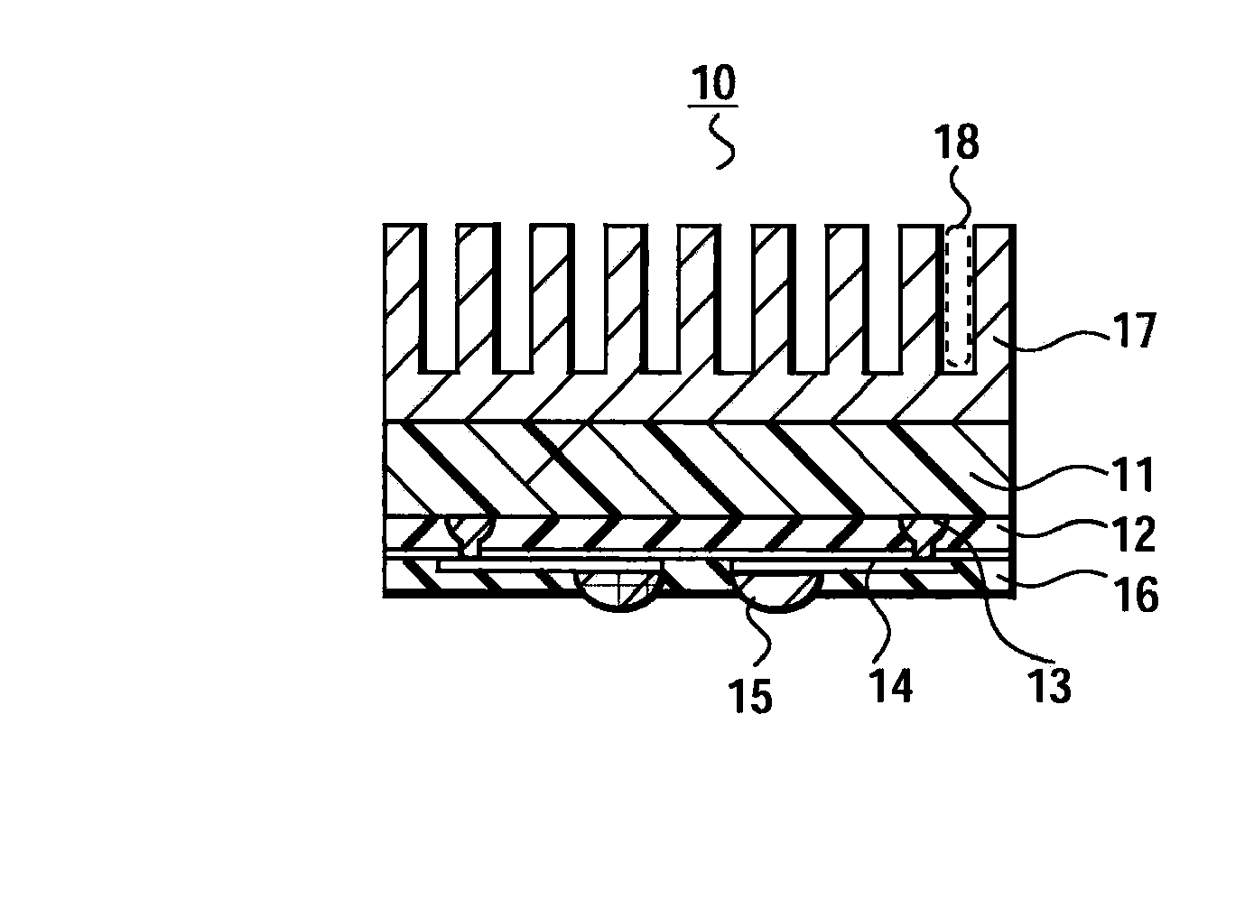
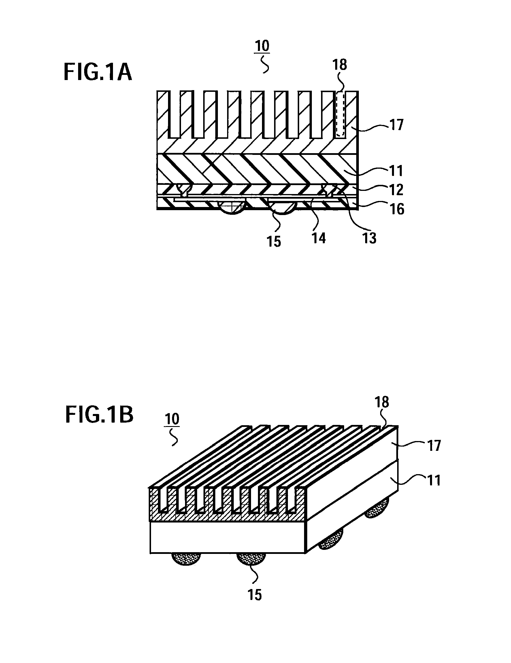
[0024] First, with reference to FIGS. 1A and 1B, a configuration of a semiconductor device 10 of this embodiment will be described. FIG. 1A is a cross-sectional view of the semiconductor device 10, and FIG. 1B is a perspective view thereof.

[0025] With reference to FIGS. 1A and 1B, the semiconductor device 10 includes: a semiconductor substrate 11; a heat sink 17 (radiator) mounted on an upper surface (a second principal surface) of the semiconductor substrate 11; wirings 14 formed on a lower surface (a first principal surface) of the semiconductor substrate 11; and the like.

[0026] The semiconductor substrate 11 is made of, for example, a semiconductor material such as silicon, and circuit elements are formed therein by a diffusion step. For example, a bipolar transistor, a MOSFET, a diode, a memory and the like are formed in the semiconductor substrate 11. A thickness of the semiconductor substrate 11 is, for example, about 25 μm to 500 μm (for example, about 50 μm). In this embod...

second embodiment

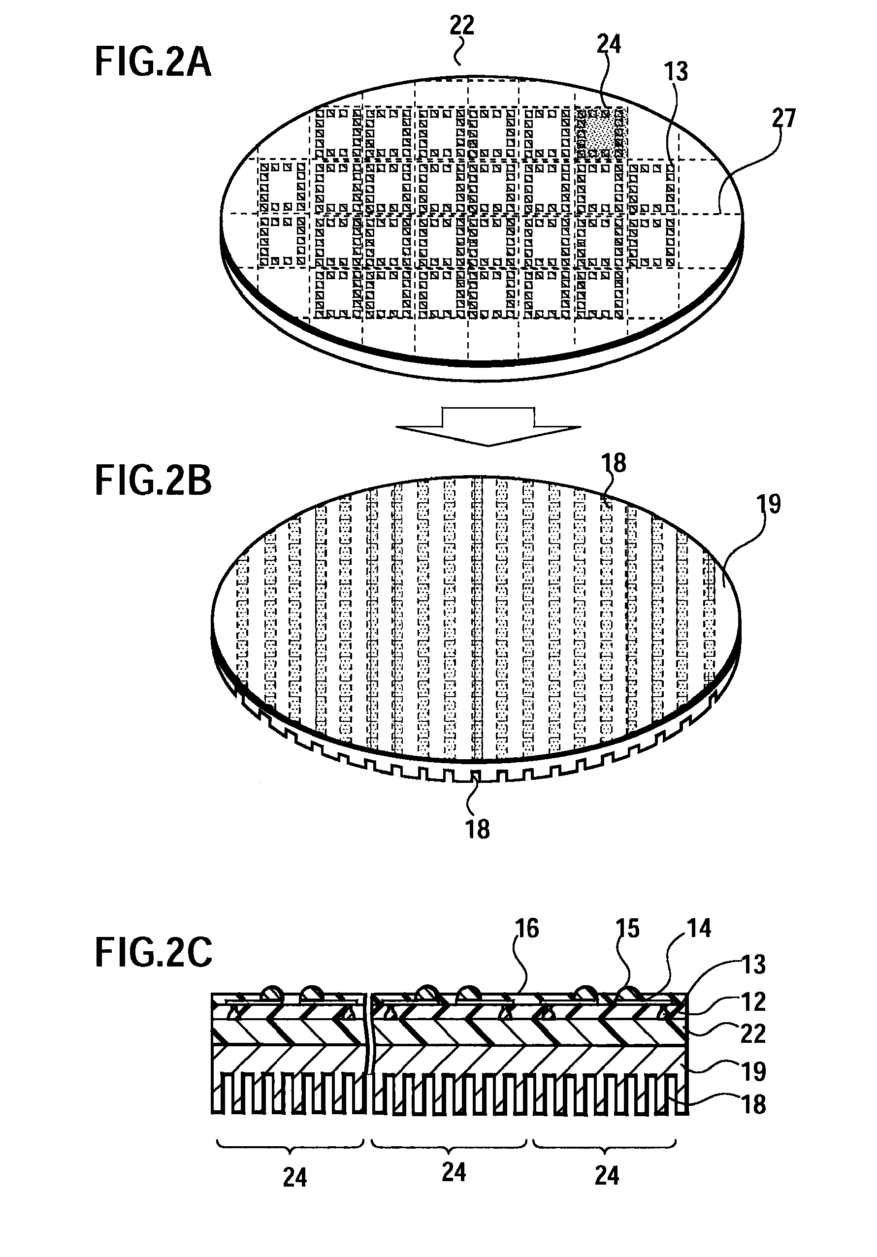
[0034] In this embodiment, with reference to FIGS. 2 to 4, description will be given of a method for manufacturing the semiconductor device having the configuration described in the first embodiment.

[0035] With reference to FIG. 2A, a semiconductor wafer 22 includes an upper surface (a first principal surface), on which electrodes 13 and the like are formed, and a flat lower surface (a second principal surface). Furthermore, on the semiconductor wafer 22, a number of (for example, a few hundred of) semiconductor device parts 24 are formed in a matrix pattern. The semiconductor device parts 24 are defined by dicing lines 27 which are provided in a lattice pattern. Here, each of the semiconductor device parts 24 is a part to become one semiconductor device. In each of the semiconductor device parts 24, predetermined circuit elements (active regions) are formed inside the semiconductor wafer 22, and the electrodes 13 connected to the elements are arranged in a peripheral portion of th...

third embodiment

[0055] With reference to FIGS. 5A to 5C, description will be given of a method for manufacturing a semiconductor device according to another embodiment. The manufacturing method of this embodiment is different from that of the second embodiment in a point that a part of a dicing sheet is left as a radiator in the semiconductor device. In the other points, this embodiment is the same as the second embodiment described above.

[0056] With reference to FIG. 5A, first, a semiconductor wafer 22 having a number of semiconductor device parts 24 formed thereon by a diffusion step and the like is attached to a dicing sheet 21 with a second adhesion layer 20 interposed therebetween.

[0057] The dicing sheet 21 includes a first sheet 31 and a second sheet 32, which are bonded to each other with a first adhesion layer 28 interposed therebetween. A boundary surface between the first and second sheets 31 and 32 is set to be an uneven surface. Here, the uneven surface has a cross-section with rectan...


PUM


Abstract

A semiconductor device includes: a semiconductor substrate; a heat sink mounted on an upper surface of the semiconductor substrate; wirings formed on a lower surface of the semiconductor substrate; and the like. The heat sink is mounted on the upper surface of the semiconductor substrate, and a planar size thereof is approximately the same as that of the semiconductor substrate. Moreover, the heat sink has a thickness of 500 μm to 2 mm, and may be formed to be thicker than the semiconductor substrate. By using the heat sink to reinforce the substrate, a thickness of the semiconductor substrate can be reduced to, for example, about 50 μm. As a result, a thickness of the entire semiconductor device can be reduced.

Description

[0001] Priority is claimed to Japanese Patent Application Number JP2006-091170 filed on Mar. 29, 2006, the disclosures of which are incorporated herein by reference in its entirety. BACKGROUND OF THE INVENTION [0002] 1. Field of the Invention [0003] The present invention relates to a semiconductor device and a manufacturing method thereof, and particularly relates to a semiconductor device having improved heat radiation properties and a manufacturing method thereof. [0004] 2. Description of the Prior Art [0005] As to circuit devices set in electronic equipment, reduction in size, thickness and weight thereof has heretofore been demanded for adoption thereof in portable telephones, portable computers and the like. In order to satisfy these conditions, a semiconductor device called a CSP (Chip Scale Package) has been developed, which has the same size as that of a semiconductor element to be built thereinto. [0006] Among the CSPs, there is a particularly small WLP (Wafer Level Package...

Claims


Application Information

Patent Timeline
IPC IPC(8): H01L23/34
CPCH01L23/367H01L2224/16H01L2224/73253H01L2924/13091H01L2924/01019H01L2924/1305H01L21/78H01L2924/00
Inventor YOSHIMI, HIDEAKIUMEMOTO, MITSUOONDA, KAZUMIHORINAKA, KAZUMI
Owner SEMICON COMPONENTS IND LLC
Why Eureka
Try Eureka