Semiconductor Module with Serial Bus Connection to Multiple Dies

a technology of serial bus and semiconductors, applied in the direction of printed circuit manufacturing, printed circuit aspects, electrical apparatus construction details, etc., can solve the problems of increasing the weight of the module, requiring separate heat spreaders to be placed, and adding significant weight to the module, so as to reduce the need for additional circuit board space, and reduce the complexity of circuit board layout and cost

Inactive Publication Date: 2007-10-04
HABA BELGACEM
View PDF12 Cites 3 Cited by
  • Summary
  • Abstract
  • Description
  • Claims
  • Application Information

AI Technical Summary

Benefits of technology

[0014] The termination resistor coupled to the semiconductors substantially reduces any degradation of the signal caused by a load placed on the signal from electrical leads, as the signal is not being split as is the case with stubs in existing semiconductor modules. Furthermore, by incorporating the termination resistor into the semiconductor module, the need for a termination resistor on the printed circuit board is eliminated, thereby reducing the need for additional circuit board space, and deceasing circuit board layout complexity and cost.

Problems solved by technology

A problem with in-line memory modules is that adding more chips to the circuit board spreads out the placement of the chips on the circuit card and therefore requires reconfiguration of the circuit card connectors and their associated connections on the motherboard, which means replacing the memory card and in some cases the motherboard.
Another problem with current in-line memory modules is that a separate heat spreader must be positioned across a set of memory chips.
The heat spreader adds cost to the assembly process and adds significant weight to the module.
However, each successive electrical lead slightly degrades the signal, by placing a load on the signal.
The longer the electrical lead, the more the signal degradation.
Therefore, existing MCMs can only handle a maximum of approximately thirty two semiconductors connected to a single transmission channel before the signal has degraded to an unusable form.

Method used


Image

  • Semiconductor Module with Serial Bus Connection to Multiple Dies
  • Semiconductor Module with Serial Bus Connection to Multiple Dies
  • Semiconductor Module with Serial Bus Connection to Multiple Dies

Examples


Embodiment Construction

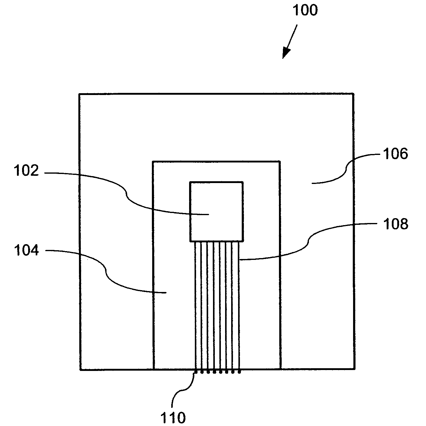
[0032]FIG. 1 is a front view of a semiconductor module 100 according to an embodiment of the invention. A semiconductor 102 is electrically connected to a plurality of traces or electrically conductive leads 108 by any conventional method such as wire bonding or thermocompression bonding. The electrically conductive leads 108 may be incorporated into flexible circuitry or tape 104, which preferably consists of copper traces within a thin dielectric substrate (such as polyimide, epoxy, etc.).

[0033] As shown in FIG. 1, the flexible circuitry 104 may be bonded, with an epoxy or the like, directly onto the side of the heat spreader 106. The heat spreader 106 is preferably made from a material with good heat dissipation properties, such as a metal.

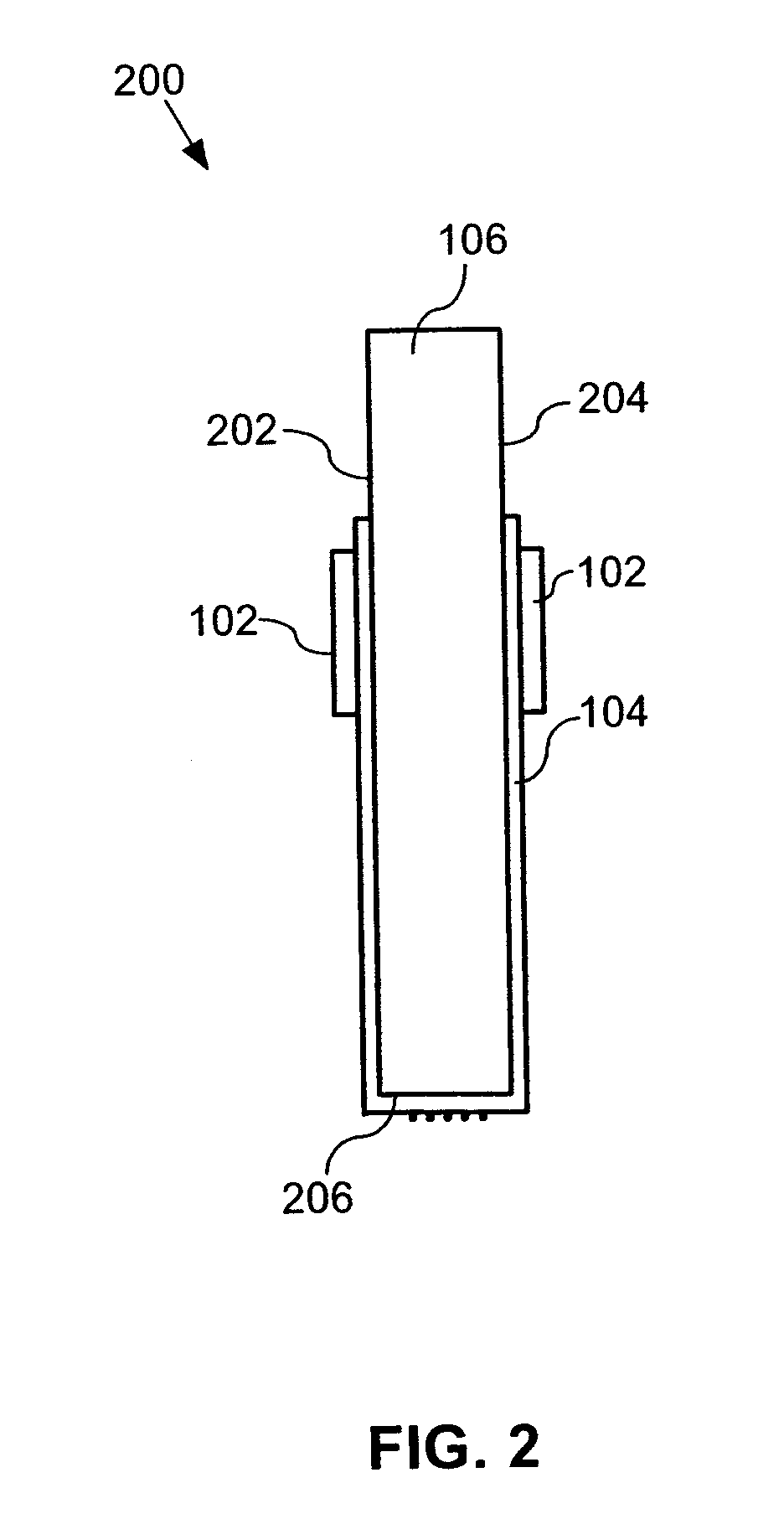
[0034] In a preferred embodiment, two semiconductors 102 are positioned on opposing sides of the heat spreader 106. The leads 108 preferably run the length of each sides of the heat spreader 106, culminating at electrical contact points 110 a...


PUM


Abstract

The semiconductor module includes a heat spreader, two semiconductors that include circuitry, a termination resistor, an array of electrical contact points, and a plurality of electrically conductive leads. The semiconductors are thermally coupled to the heat spreader. The terminator resistor is electrically coupled to the circuitry of at least one of the semiconductors. The array of electrical contact points are coupled to the heat spreader. The conductive leads are electrically connected to the semiconductors and the array of electrical contact points. At least one of the leads is common to both of the semiconductors.

Description

[0001] This application claims priority to and is a continuation of U.S. Ser. No. 11 / 398,458 filed on Feb. 7, 2002 entitled “Semiconductor Module With Serial Bus Connection To Multiple Dies”, which is a reissue of U.S. Pat. No. 6,833,984, which is a continuation in part of U.S. Ser. No. 09 / 564,064 filed on May 3, 2000 entitled “Semiconductor Module with Imbedded Heat Spreader”, all of which are incorporated by reference herein in their entirety.TECHNICAL FIELD [0002] The present invention relates generally to semiconductor modules and in particular to a semiconductor module that allows for more efficient interconnection between the semiconductor module and a computing device's transmission channel. BACKGROUND OF THE INVENTION [0003] The semiconductor industry is constantly producing smaller and more complex semiconductors, sometimes called integrated circuits or chips. This trend has brought about the need for smaller chip packages with smaller footprints, higher lead counts, and be...

Claims


Application Information

Patent Timeline
Patent Type & Authority Applications(United States)
IPC IPC(8): H05K7/20H01L23/36H01L23/538H01L25/065
CPCH01L23/36H01L23/367H01L2924/12032H01L23/4985H01L23/5387H01L23/552H01L23/647H01L24/86H01L25/0655H01L25/0657H01L2225/06517H01L2225/0652H01L2225/06527H01L2225/06551H01L2225/06579H01L2225/06586H01L2225/06589H01L2924/14H01L2924/19105H01L2924/3011H01L2924/3025H05K1/0246H05K1/189H05K3/0061H05K2201/056H05K2201/09445H05K2201/10022H05K2201/1056H05K2201/10674H01L2924/00
Inventor HABA, BELGACEM
Owner HABA BELGACEM
Why Eureka
Try Eureka