[0012] An
advantage of the present invention is that it provides an optical
path switching device and method in which no electric circuits or mechanically
moving parts are used. Such optical
path switching device and method are reliable, have excellent durability, and have no polarization dependency. Further, the optical path switching angles and directions can be freely set. Other advantages of the present invention are that attenuation of the
signal light intensity is reduced, and that the device and method can be used in a multi-linked manner.
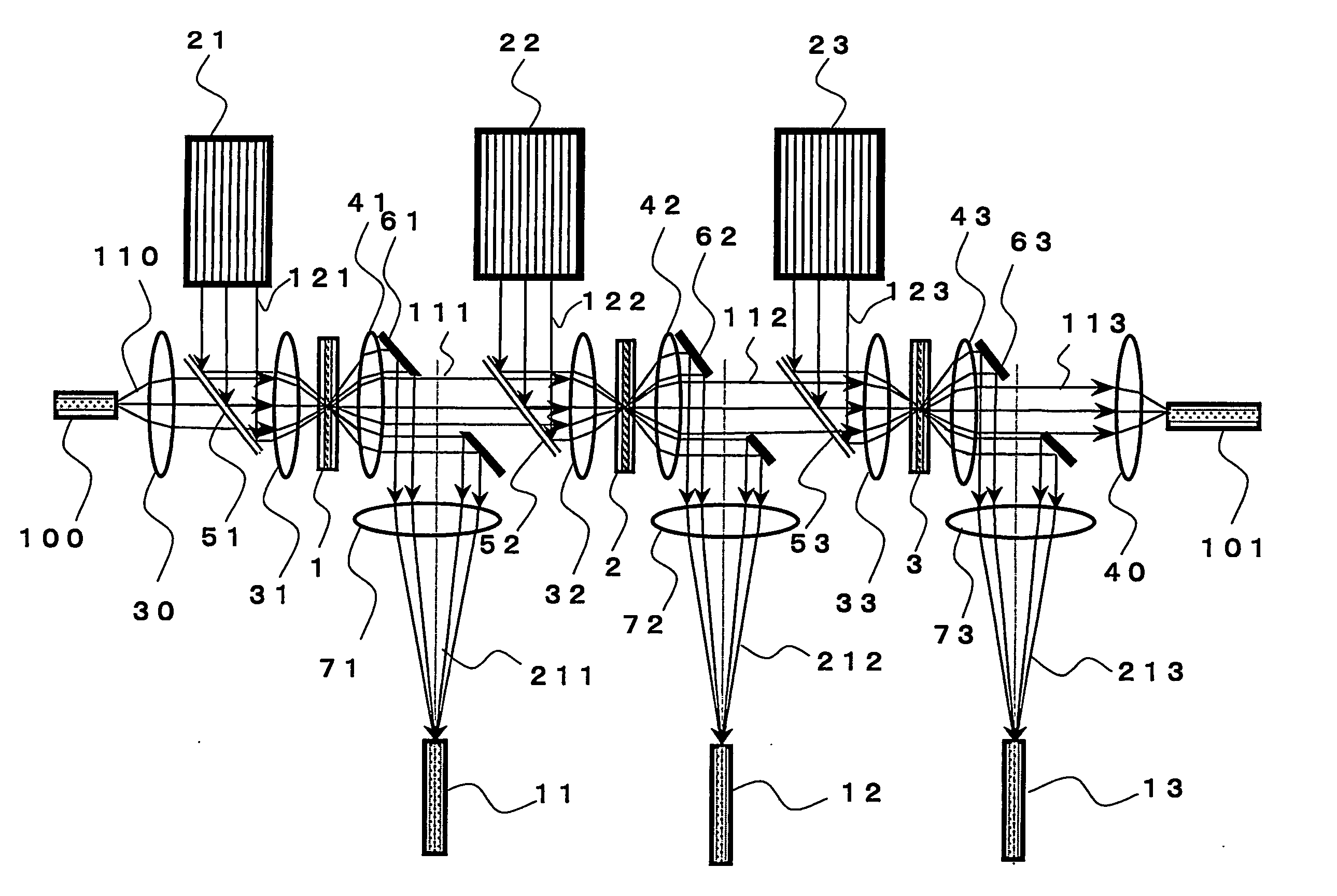
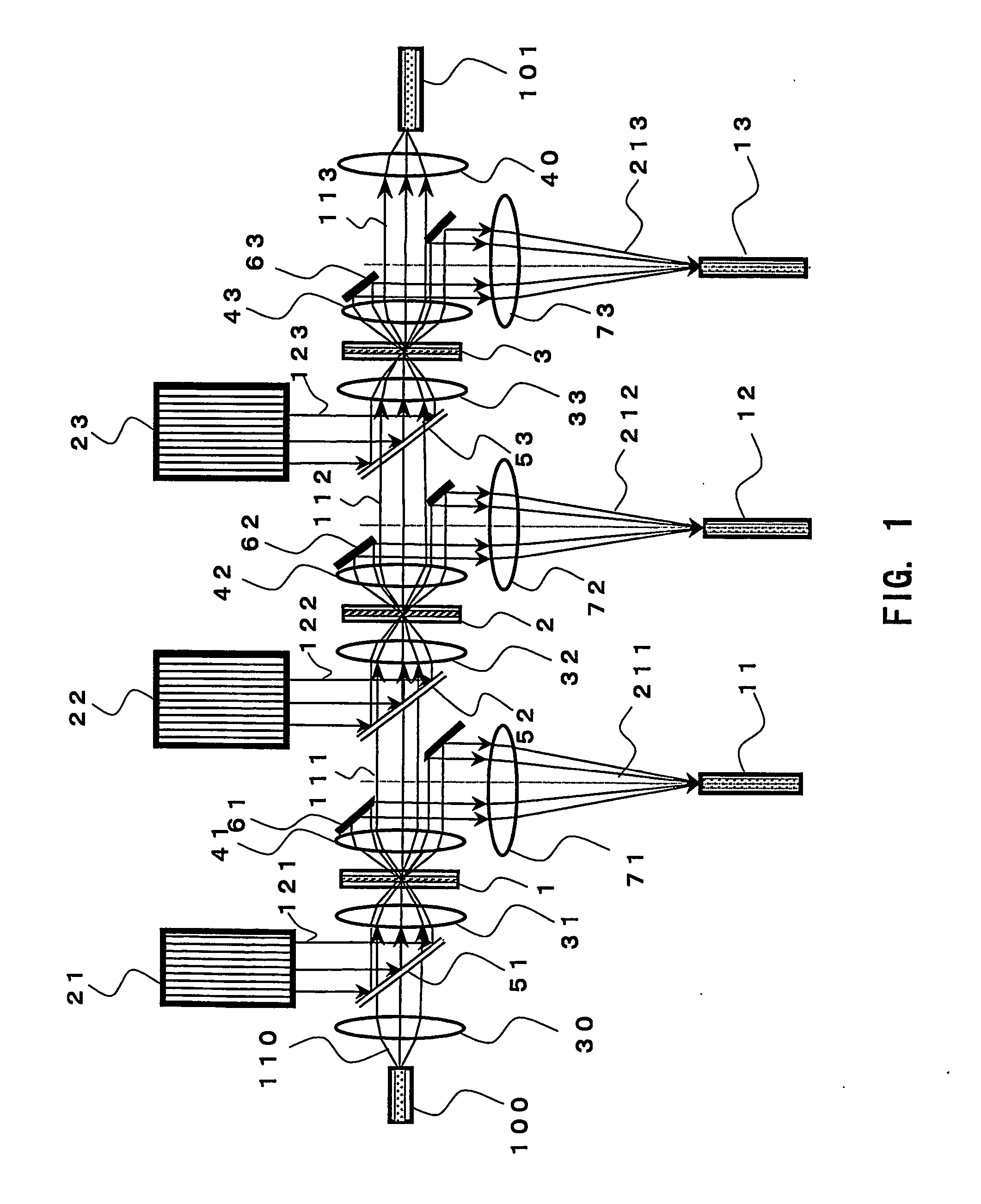
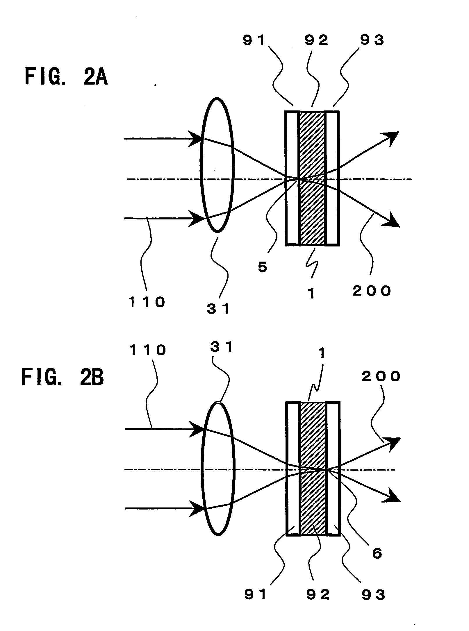
[0013] To accomplish the above advantages, an optical path switching device according to the present invention comprises a light absorption layer film arranged such that at least a control light focuses on the light absorption layer film, means for converging and irradiating on the light absorption layer film each of a control light having a wavelength selected from a
wavelength band which is absorbed by the light absorption layer film and a
signal light having a wavelength selected from a
wavelength band which is not absorbed by the light absorption layer film, and a thermal lens forming element including the light absorption layer film. A thermal lens is reversibly formed according to a distribution of refraction index created by a temperature increase generated in and around an area of the light absorption layer film in which the control light is absorbed. When the control light is not irradiated and the thermal lens is not formed, the converged
signal light is output while spreading at a normal spread angle, and, when the control light is irradiated and the thermal lens is formed in the vicinity of an incident surface of the light absorption layer film, the converged signal light is output while spreading at a spread angle greater than the normal spread angle. In this manner, the thermal lens forming element allows the spread angle of the output signal light to be changed according to whether or not the control light is irradiated. The optical path switching device further comprises a mirror for changing an optical path. The mirror includes a hole through which passes, when the control light is not irradiated and the thermal lens is not formed, the signal light output from the thermal lens forming element at the normal spread angle as is or after the spread angle is changed by a
receiver lens. The mirror further includes means for reflecting, when the control light is irradiated and the thermal lens is formed in the vicinity of an incident surface of the light absorption layer film, the signal light output from the thermal lens forming element at the normal spread angle as is or after the spread angle is changed by the
receiver lens.
[0014] The
receiver lens is used to change the signal light output from the thermal lens forming element at the normal spread angle or at the spread angle greater than the normal spread angle into a substantially “parallel” beam. However, it should be noted that the resulting beam need not be completely parallel.
[0015] To accomplish the above advantages, another optical path switching device according to the present invention comprises a light absorption layer film arranged such that at least a control light focuses on the light absorption layer film, means for converging and irradiating on the light absorption layer film each of a control light having a wavelength selected from a wavelength band which is absorbed by the light absorption layer film and a signal light having a wavelength selected from a wavelength band which is not absorbed by the light absorption layer film, and a thermal lens forming element including the light absorption layer film. A thermal lens is reversibly formed according to a distribution of refraction index created by a temperature increase generated in and around an area of the light absorption layer film in which the control light is absorbed. When the control light is irradiated and the thermal lens is formed in the vicinity of an output surface of the light absorption layer film, the converged signal light is output as converged, and, when the control light is not irradiated and the thermal lens is not formed, the converged signal light is output at a normal spread angle. In this manner, the thermal lens forming element allows the spread angle of the output signal light to be changed according to whether or not the control light is irradiated. The optical path switching device further comprises a mirror for changing an optical path. The mirror includes a hole through which passes, when the control light is irradiated and the thermal lens is formed in the vicinity of an output surface of the light absorption layer film, the converged signal light output from the thermal lens forming element. The mirror further includes means for reflecting, when the control light is not irradiated and the thermal lens is not formed, the signal light output from the thermal lens forming element at the normal spread angle as is or after being passed through a receiver lens provided for changing the spread angle.
[0016] To accomplish the above advantages, an optical path switching method according to the present invention comprises converging and irradiating, on a light absorption layer film provided in a thermal lens forming element including at least the light absorption layer film, each of a control light having a wavelength selected from a wavelength band which is absorbed by the light absorption layer film and a signal light having a wavelength selected from a wavelength band which is not absorbed by the light absorption layer film. Arrangement of the light absorption layer film is adjusted such that at least the control light focuses within the light absorption layer film. A thermal lens is reversibly formed according to a distribution of refraction index created by a temperature increase generated in and around an area of the light absorption layer film in which the control light is absorbed. When the control light is not irradiated and the thermal lens is not formed, the converged signal light is output from the thermal lens forming element while spreading at a normal spread angle, and, when the control light is irradiated and the thermal lens is formed in the vicinity of an incident surface of the light absorption layer film, the converged signal light is output from the thermal lens forming element while spreading at a spread angle greater than the normal spread angle. In this manner, the spread angle of the output signal light is changed according to whether or not the control light is irradiated. Subsequently, when the control light is not irradiated and the thermal lens is not formed, the signal light output from the thermal lens forming element at the normal spread angle is, as is or after the spread angle is changed by a receiver lens, passes through a hole in a mirror with a hole and allowed to proceed straight. On the other hand, when the control light is irradiated and the thermal lens is formed in the vicinity of an incident surface of the light absorption layer film, the signal light output from the thermal lens forming element while spreading at the spread angle greater than the normal spread angle is, as is or after the spread angle is changed by the receiver lens, reflected using a reflection surface of the mirror with the hole so as to change an optical path.
[0017] To accomplish the above advantages, another optical path switching method according to the present invention comprises converging and irradiating, on a light absorption layer film provided in a thermal lens forming element including at least the light absorption layer film, each of a control light having a wavelength selected from a wavelength band which is absorbed by the light absorption layer film and a signal light having a wavelength selected from a wavelength band which is not absorbed by the light absorption layer film. Arrangement of the light absorption layer film is adjusted such that at least the control light focuses within the light absorption layer film. A thermal lens is reversibly formed according to a distribution of refraction index created by a temperature increase generated in and around an area of the light absorption layer film in which the control light is absorbed. When the control light is irradiated and the thermal lens is formed in the vicinity of an output surface of the light absorption layer film, the converged signal light is output from the thermal lens forming element as converged, and, when the control light is not irradiated and the thermal lens is not formed, the converged signal light is output from the thermal lens forming element at a normal spread angle. In this manner, the spread angle of the output signal light is changed according to whether or not the control light is irradiated. Subsequently, when the control light is irradiated and the thermal lens is formed in the vicinity of the output surface of the light absorption layer film, the converged signal light output from the thermal lens forming element passes through a hole in a mirror with a hole and allowed to proceed straight. On the other hand, when the control light is not irradiated and the thermal lens is not formed, the signal light output from the thermal lens forming element at the normal spread angle is, as is or after the spread angle is changed by a receiver lens, reflected using a reflection surface of the mirror with the hole so as to change an optical path.

