Carbon Nanotube Device and Process for Producing the Same

a carbon nanotube and process technology, applied in the field of carbon nanotube devices and processes, can solve the problems of difficult search for an appropriate support condition of a catalyst, large mixing of catalysts, and aggregation and coarsening under, and achieve the effects of reducing the space of the layer, reducing the mixing of impurities in carbon nanotubes, and simplifying the process

Inactive Publication Date: 2007-10-04
DAINIPPON SCREEN MTG CO LTD +1
View PDF4 Cites 5 Cited by
  • Summary
  • Abstract
  • Description
  • Claims
  • Application Information

AI Technical Summary

Benefits of technology

[0028] The invention is useful for a process for fabricating a carbon nanotube device which causes good carbon nanotubes to grow up at an arbitrary location on a substrate.
[0029] It is important as an analysis method which finds out the best catalyst support condition from the broad range of metal deposition rates at one experiment despite a reaction condition, and the values as a production process and a production device are high.
[0030] The carbon nanotubes themselves grown on the substrate can select the nominal thickness distribution pattern of a catalyst substance formed on the substrate, the carbon nanotubes formed at the center of the pattern can entwine with one another, can grow in the substrate vertical direction, not in the substrate surface horizontal direction, thereby making it possible to fabricating a device formed in a needle-like shape.
[0031] At this time, because the needle of carbon nanotubes is formed at the bottom portion of the space opened in the substrate vertical direction in the layer on the substrate, a device with this structure can be directly used as an electrode of a field emission display, or can be used as the probe of a scanning probe microscope or an information reading / writing device of a recording device by eliminating the layer having the space.
[0032] In particular, because catalyst support in an appropriate amount becomes possible, mixing of impurities in carbon nanotubes is extremely less, and this is very important for the application of the device.
[0033] Further, when a fine pattern is formed in a multilayer structure on the substrate using photolithography, an array of carbon nanotubes can be formed. Multilayer structure formation is somehow complicated, but formation of a fine pattern (down to several tens nm) becomes possible, this enables densification, and more particularly, a fine structure used as a mask can be directly used as a device structure in a field emission electron source, so that there is an advantage such that a process is simplified.

Problems solved by technology

In using the metal nanoparticle catalysts made beforehand, however, there is a problem such that the metal nanoparticle catalysts may cause aggregation and coarsening under a high temperature of synthesizing carbon nanotubes.
The scheme of spontaneously forming the metal nanoparticle catalysts has a problem such that searching of an appropriate support condition of a catalyst is difficult.
In any schemes, however, only a part of a metal on the substrate functions as a catalyst, and there is a problem such that lots of catalysts are mixed as impurities in carbon nanotubes.
According to the scheme of [Patent Literature 1], however, because the controllability of the direction of the carbon nanotubes which form a pattern is low so that only a part of the carbon nanotubes function as an electrode, and because electrical connection between carbon nanotubes and the substrate is bad, the property of a device is not always good from the standpoint of life duration and power consumption.

Method used


Image

  • Carbon Nanotube Device and Process for Producing the Same
  • Carbon Nanotube Device and Process for Producing the Same
  • Carbon Nanotube Device and Process for Producing the Same

Examples


first embodiment

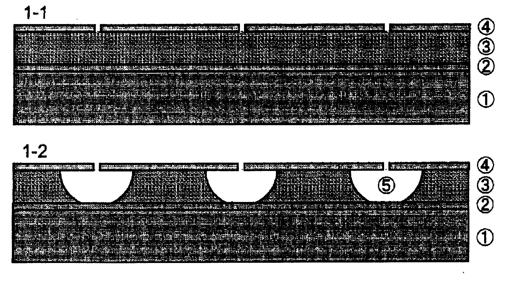
[0047]FIG. 1 is a cross-sectional view illustrating the structure of a carbon nanotube device in production steps according to an embodiment of the invention.

[0048] The carbon nanotube device of the embodiment has a conductive film (2) formed on a substrate (1), an insulating film (3) with holes (5) formed on the conductive film, and a coating film (4) formed on the insulating film. Catalyst substances (6) are used in the production steps, and spiny carbon nanotube aggregates (7) extend from the conductive film (2) exposed with respect to the holes (5) toward the tiny openings of the coating film (4).

[0049] Note that the coating film (4) may be omitted. The substrate (1) and the conductive film (2) may be considered as one “substrate” as a whole. In this case, the conductive film (2) which is a surface of the “substrate” is exposed by the holes (5). In a case where it is considered that the substrate (1) and the conductive film (2) are separate demonstratively, the holes (5) also ...

second embodiment

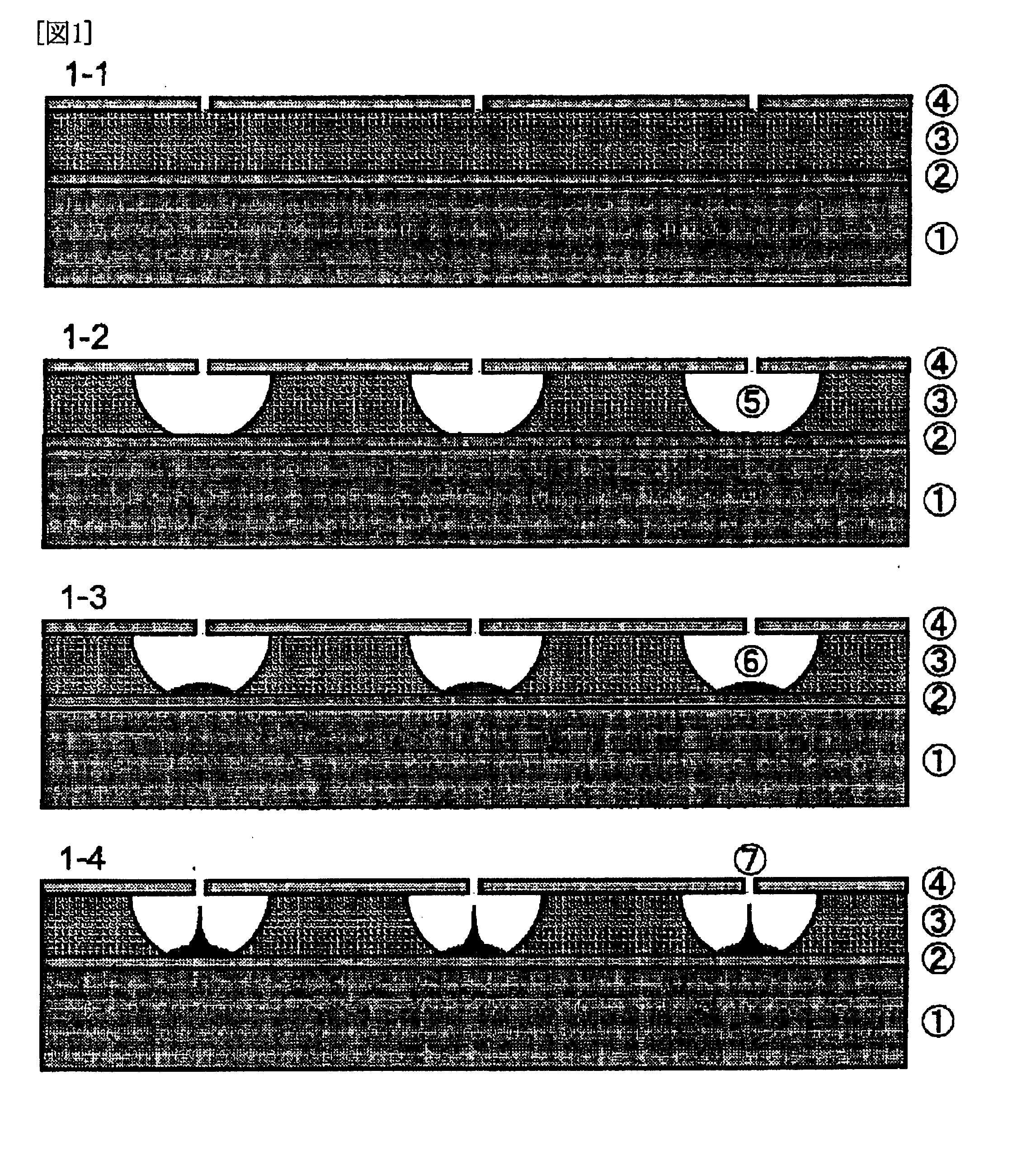
[0100]FIG. 4 is an explanatory diagram illustrating a modified example of the foregoing embodiment. An explanation will be given with reference to this figure. A carbon nanotube device of the embodiment has the conductive film (2) formed on the substrate (1), the insulating film (3) formed thereon, and the coating film (4) formed thereon. The holes (5) in the embodiment penetrate both insulating film (3) and conductive film (2), and the substrate (1) is exposed with respect to the holes (5).

[0101] The catalyst substances (6) are used in the production steps, and the spiny single-walled carbon nanotube aggregates (7) extend from the conductive film (2) exposed with respect to the holes (5) toward the tiny openings of the coating film (4).

[0102] As typical materials, a silicon substrate with an oxide film is used for the substrate (1), an Mo film (Mo, W, or the like) is used for the conductive film (2), a silicon dioxide film is used for the insulating film (3), a conductive chrome ...

third embodiment

[0115]FIG. 5 is an explanatory diagram illustrating a modified example of the foregoing embodiments. A carbon nanotube device of the embodiment has the conductive film (2) formed on the substrate (1), the insulating film (3) with the holes (5) formed thereon, and the coating film (4) formed thereon. In the production steps, the catalyst substances (6) are used, and the spiny single-walled carbon nanotube aggregates (7) extend from the conductive film (2) exposed with respect to the holes (5) toward the openings of the coating film (4).

[0116] As typical materials, a silicon substrate with an oxide film is used for the substrate (1), an Mo film (Mo, W, or the like) is used for the conductive film (2), a silicon dioxide film is used for the insulating film (3), a conductive chrome film is used for the coating film (4), and silicon dioxide and Co, Fe, Ni, Mo, or the like is used for the catalyst substance (6).

[0117] Although major part of the invention is the same as that of the embod...


PUM

PropertyMeasurementUnit
temperatureaaaaaaaaaa
thicknessaaaaaaaaaa

Abstract

A carbon nanotube device has a substrate (1), a layer (3) having a space (5) which penetrates in the vertical direction of the substrate (1), and carbon nanotubes (7) formed on the surface of the substrate facing the space (5) in such a manner as to have number density distributions successively changed according to the distances from the center of the space (5), the supply amount of catalyst substances is diluted by supplying the catalyst substances through an opening of a coating film (4) opposite to the substrate (1) and the hole (5), a catalyst having a nominal thickness distribution according to the way how the space (5) appears is formed on the substrate (1) facing the space (5), and a carbon source is supplied, thereby forming carbon nanotubes having the number density distribution are formed on the substrate (1).

Description

TECHNICAL FIELD [0001] The present invention relates to a carbon nanotube device and a process for producing the same. [0002] More particularly, provided are a carbon nanotube device that has carbon nanotubes at a specific number density distribution in a layer having a space which penetrates in a substrate vertical direction on a substrate, and a process for producing a carbon nanotube device which supports nano-sized catalyst particles under a condition such that the catalyst particles do not cause coarsening, has good quality carbon nanotubes, enables fine structure control, and is suitable for the structure of a field emission electron source. BACKGROUND [0003] To produce a carbon nanotube device having carbon nanotubes distributed on a substrate, it is necessary to provide metal nanoparticle catalysts on the substrate. Such a technique is disclosed in the following literatures. [0004] Non Patent Literature 1: kinloch, I. A.; Shaffer, M. S. P.; Lam, Y. M.; Windle, A. H. Carbon 2...

Claims


Application Information

Patent Timeline
Patent Type & Authority Applications(United States)
IPC IPC(8): H01J9/02
CPCB82Y10/00H01J2201/30469H01J31/127H01J29/04B82B3/0009B82B3/0014B82Y40/00C01B32/162
Inventor NODA, SUGURU
Owner DAINIPPON SCREEN MTG CO LTD
Why Eureka
Try Eureka