Roughness reducing film at interface, materials for forming roughness reducing film at interface, wiring layer and semiconductor device using the same, and method for manufacturing semiconductor device

a technology of roughness reducing film and roughness, which is applied in the direction of semiconductor devices, semiconductor device details, electrical apparatus, etc., to achieve the effects of high tddb resistance, high reliability of semiconductors, and small electric power consumption

Active Publication Date: 2007-10-04
FUJITSU LTD
View PDF7 Cites 12 Cited by
  • Summary
  • Abstract
  • Description
  • Claims
  • Application Information

AI Technical Summary

Benefits of technology

[0019]According to this aspect of the present invention, a highly reliable semiconductor device with a small electric power consumption can be manufactured.
[0020]According to the present invention,

Problems solved by technology

However it has been found that the reliability tests such as a TDDB test did not provide necessary properties whe

Method used


Image

  • Roughness reducing film at interface, materials for forming roughness reducing film at interface, wiring layer and semiconductor device using the same, and method for manufacturing semiconductor device
  • Roughness reducing film at interface, materials for forming roughness reducing film at interface, wiring layer and semiconductor device using the same, and method for manufacturing semiconductor device
  • Roughness reducing film at interface, materials for forming roughness reducing film at interface, wiring layer and semiconductor device using the same, and method for manufacturing semiconductor device

Examples


example 1

[0076]A coating-type low dielectric constant insulating material comprising a silicon-containing compound and having a low relative dielectric constant of 2.5 was applied onto a low-resistant substrate to a thickness of 250 nm by spin coating, the substrate was subjected to prebaking at 250° C. for three minutes, and then, cured in an electric oven under a nitrogen atmosphere at 400° C. for 30 minutes. Afterwards, etching was performed on the whole surface to a depth of 200 nm.

[0077]A sample which had not been subjected to any other treatment in the later stage was called sample 1; a sample which had been subjected only to baking at 250° C. for 1 minute without any spin coating was called sample 2; a sample which had been subjected only to spin coating with HMDS (hexamethyldisilazane) was called sample 3; a sample which had been subjected to spin coating with HMDS, followed by baking at 250° C. for 1 minute was called sample 4; a sample which had been subjected to spin coating with ...

example 2

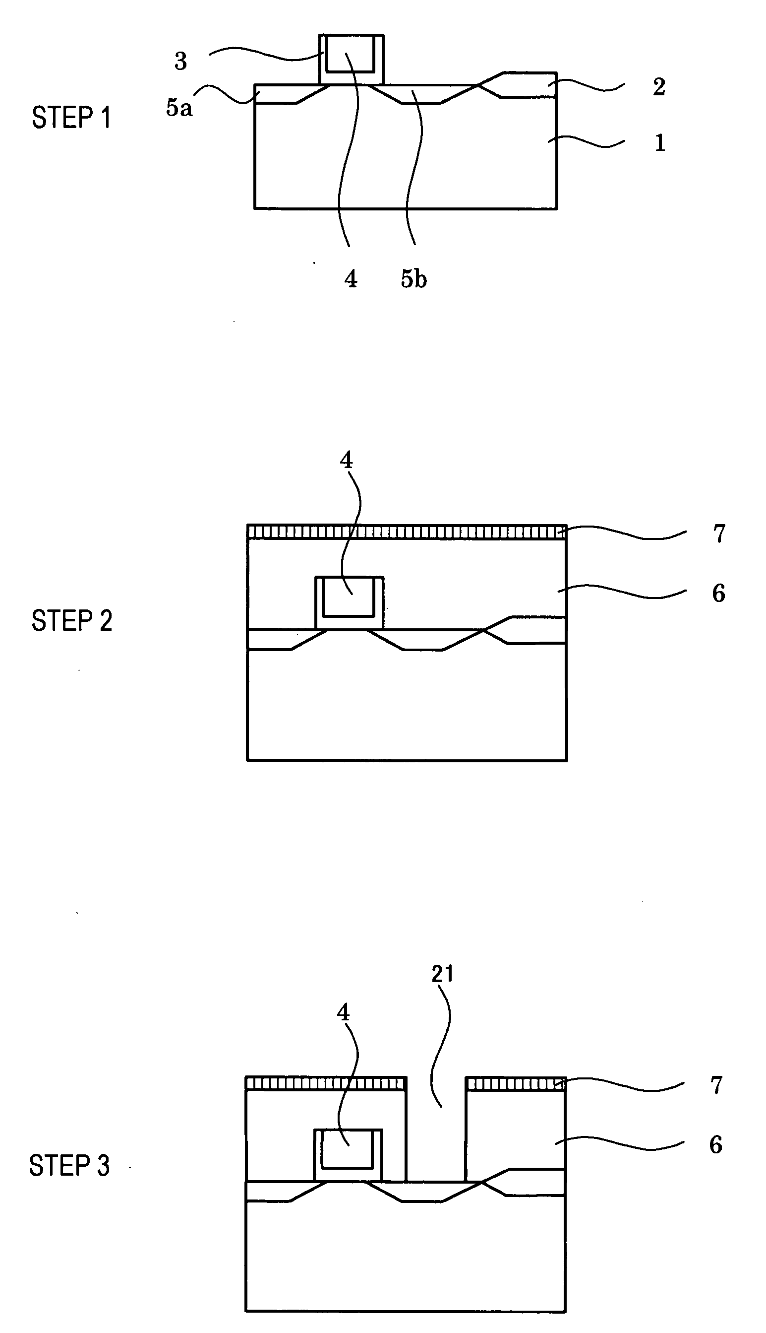
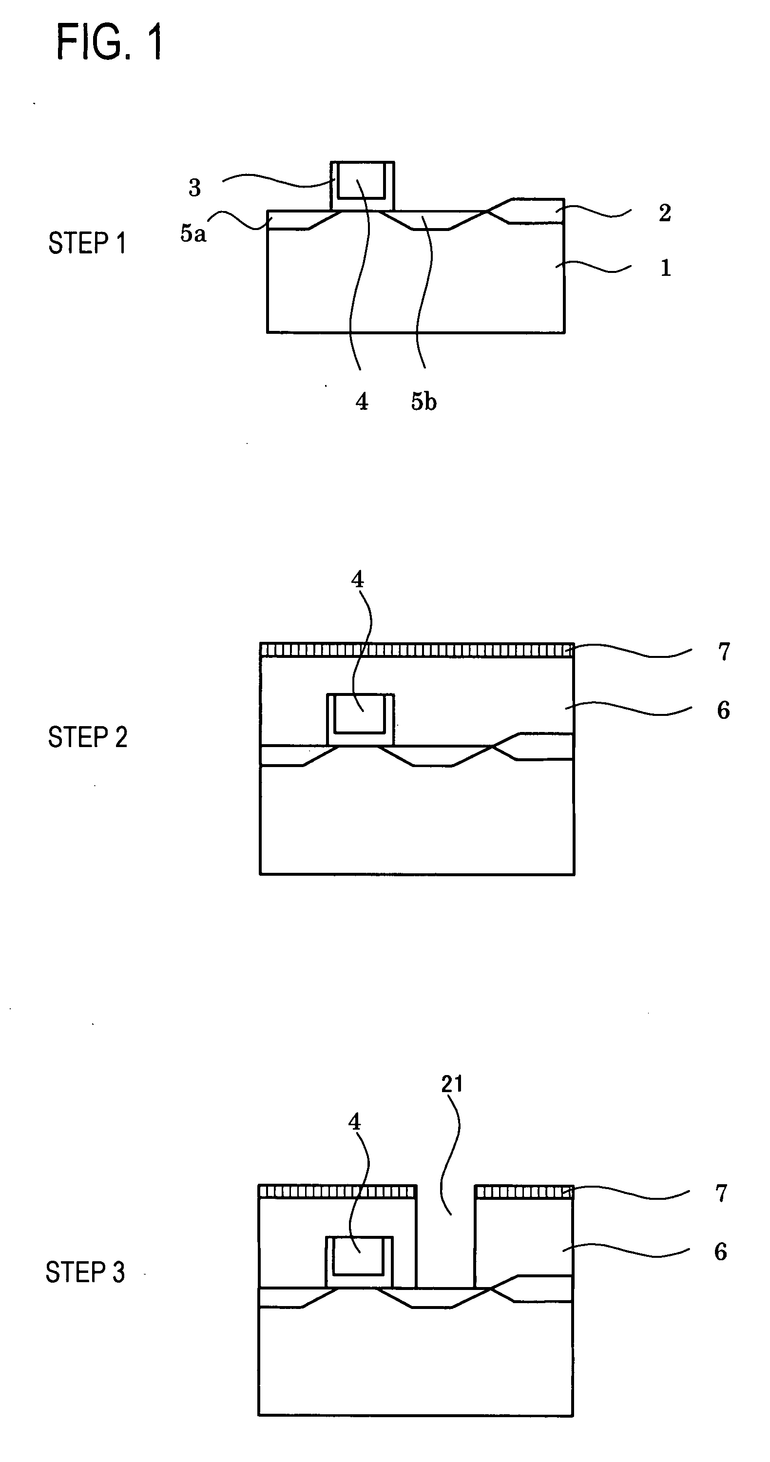
[0081]FIGS. 1-10 show how an example of a multilayer wiring structure according to the present invention is manufactured. First, on a silicon wafer 1 on which formed was a transistor layer having a gate electrode 4 with a source diffusion layer 5a, drain diffusion layer 5b and sidewall insulator film 3 (step 1) and being separated by an element separation film 2, an interlayer insulation film 6 (phosphorus glass) and a stopper film 7 were formed (step 2), and then, a contact holes 21 for leading to electrodes were formed (step 3).

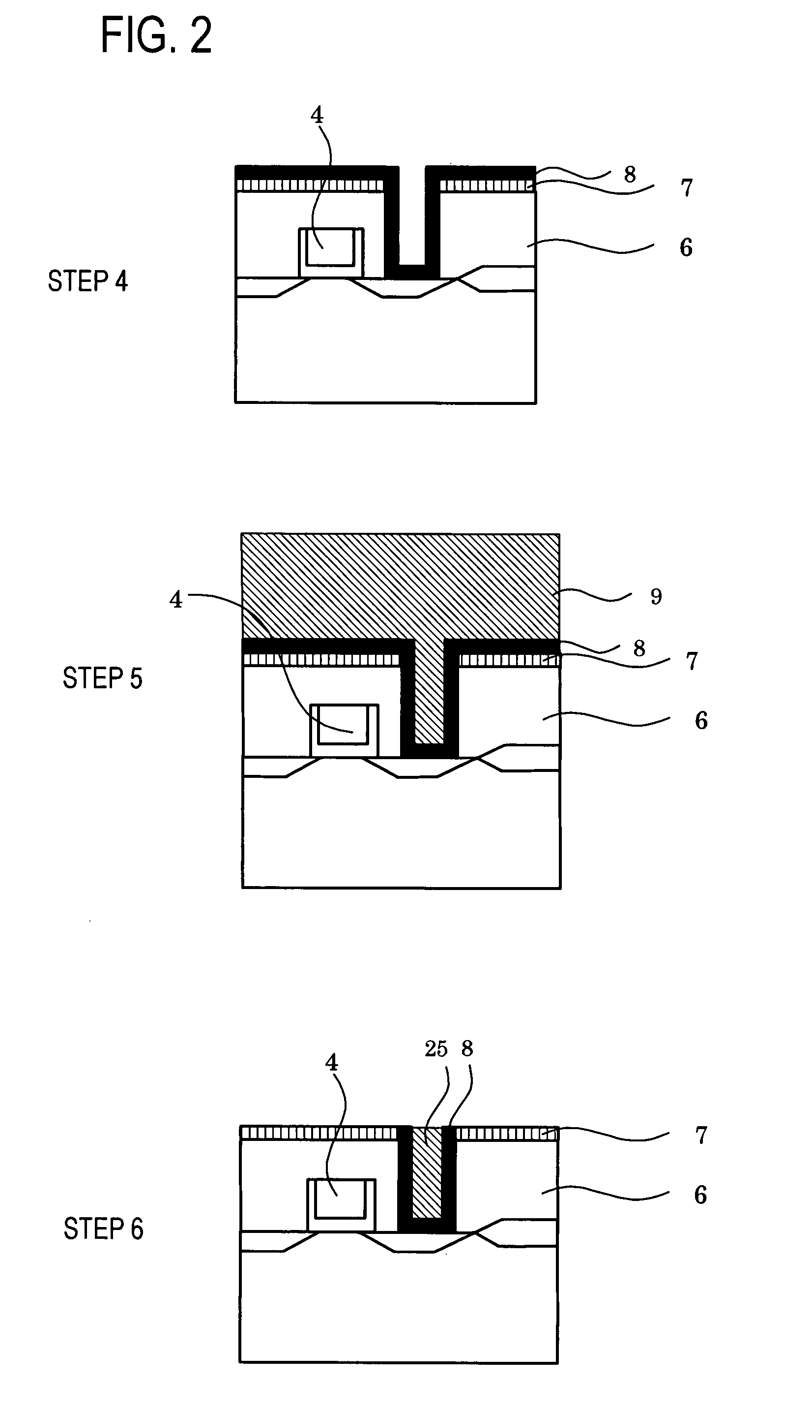
[0082]TiN 8 in a thickness of 50 nm was formed in these contact holes by a sputtering method (step 4). A mixture of WF6 and hydrogen was then reduced to form (fill in) conductor plugs 9 (step 5), the part other than via holes 25 was removed by CMP (step 6). Subsequently, a low dielectric constant coating (insulator film for wiring separation) 10 was formed so that the surface of the coating was 250 nm over the silicon wafer plane, followed by lamination of ...

example 3

[0089]A three-layer wiring structure was formed in the same way as in EXAMPLE 2, except that the interfacial roughness reducing films 12, 20 were made using sample 6 of EXAMPLE 1. The same TDDB measurement was conducted using the comb-shaped pattern for the experimentally manufactured multi-layer wiring structure. The median value until the breakdown was 426 seconds.


PUM


Abstract

Techniques for obtaining a wiring layer with a high TDDB resistance and little leakage current, and accordingly, for manufacturing a highly reliable semiconductor device with a small electric power consumption are provided, in which an interfacial roughness reducing film is formed which is in contact with an insulator film and also in contact with a wiring line on the other side surface thereof, and has an interfacial roughness between the wiring line and the interfacial roughness reducing film smaller than that between the insulator film and the interfacial roughness reducing film.

Description

CROSS-REFERENCE TO RELATED APPLICATIONS[0001]This application is based upon and claims the benefit of priority from the prior Japanese Patent Application No. 2006-091549, filed on Mar. 29, 2006, and the prior Japanese Patent Application No. 2006-349409, filed on Dec. 26, 2006, the entire contents of which are incorporated herein by reference.BACKGROUND OF THE INVENTION[0002]1. Field of the Invention[0003]The present invention relates to a technology to absorb the interfacial roughness at the interface between an insulator film and a wiring line of a semiconductor device, or the like.[0004]2. Description of the Related Art[0005]While increase of electric power consumption in a semiconductor device due to leakage current into an insulator film for a wiring layer has been known, effect of the leakage on a whole device was small in the generations when the distance between two wiring lines of a semiconductor device exceeded 1 μm. However, when the distance between two wiring lines is no...

Claims


Application Information

Patent Timeline
IPC IPC(8): H01L21/31
CPCH01L21/3105H01L21/76831H01L21/316H01L21/3121H01L21/022H01L21/02282H01L21/02126H01L21/02274H01L21/02211H01L21/02164H01L21/02167H01L21/0217H01L21/28
Inventor IMADA, TADAHIRONAKATA, YOSHIHIROYANO, EI
Owner FUJITSU LTD
Why Eureka
Try Eureka