

Transfer pick, transfer device, substrate processing apparatus and transfer pick cleaning method
- Summary
- Abstract
- Description
- Claims
- Application Information
AI Technical Summary
Benefits of technology
Problems solved by technology
Method used
Image

Examples
Embodiment Construction
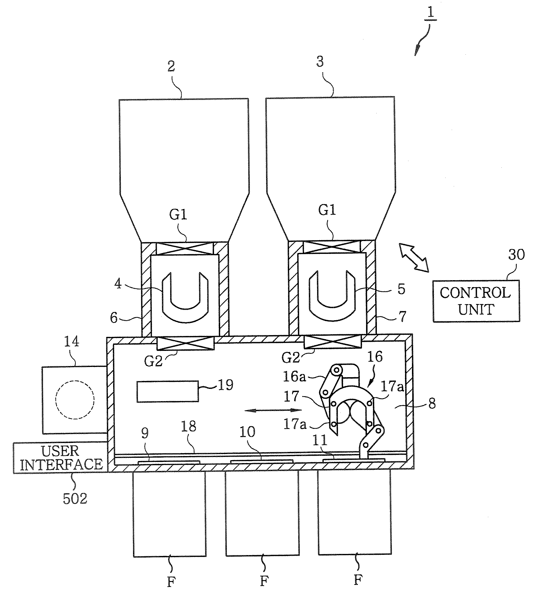
[0037]Hereinafter, embodiments of the present invention will be described in detail with reference to the accompanying drawings. FIG. 1 is a schematic horizontal sectional view showing a plasma processing device of a substrate processing apparatus in accordance with an embodiment of the present invention. The plasma process device 1 serves to process, for example, etch a semiconductor wafer W (hereinafter, referred to simply as “wafer”), which is the target substrate, under a specific vacuum level.
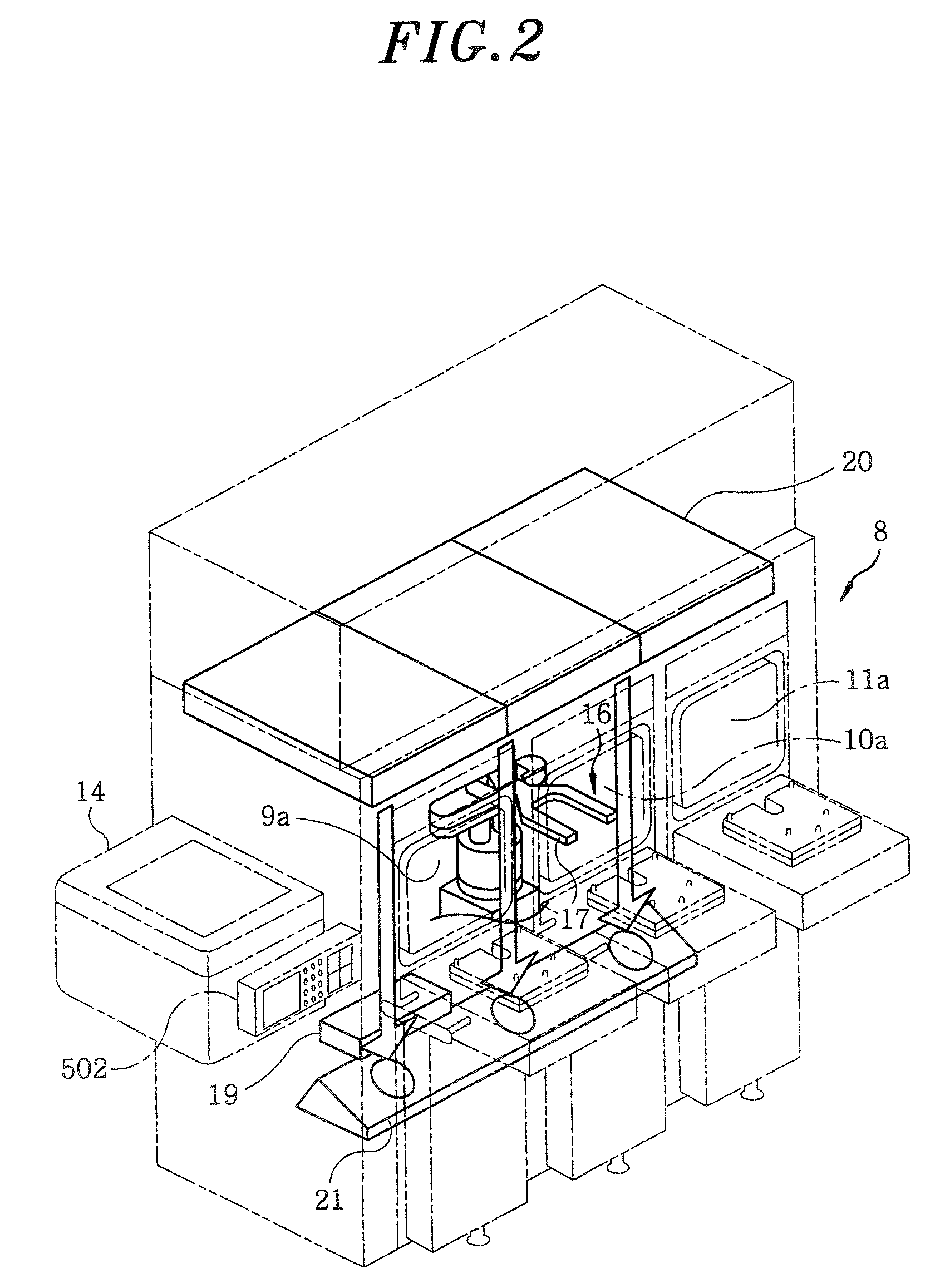
[0038]The plasma processing device 1 includes two processing units 2 and 3, and is constructed such that each of the processing units 2 and 3 can independently perform the etching process on the wafer W. Load lock chambers 6 and 7 are coupled to the processing units 2 and 3, respectively, via gate valves G1. A wafer accessing chamber 8, which is a conveyance chamber is provided at the ends of the load lock chambers 6 and 7 that are opposite of the process units 2 and 3. Three connection po...
PUM
 Abstract
Description
Claims
Application Information