Data Output Clock Selection Circuit For Quad-Data Rate Interface
a data output clock and data rate interface technology, applied in the direction of instruments, generating/distributing signals, pulse techniques, etc., can solve the problems of narrowing the frequency range even further and creating glitches, and achieve the effect of eliminating glitches
- Summary
- Abstract
- Description
- Claims
- Application Information
AI Technical Summary
Benefits of technology
Problems solved by technology
Method used
Image
Examples
Embodiment Construction
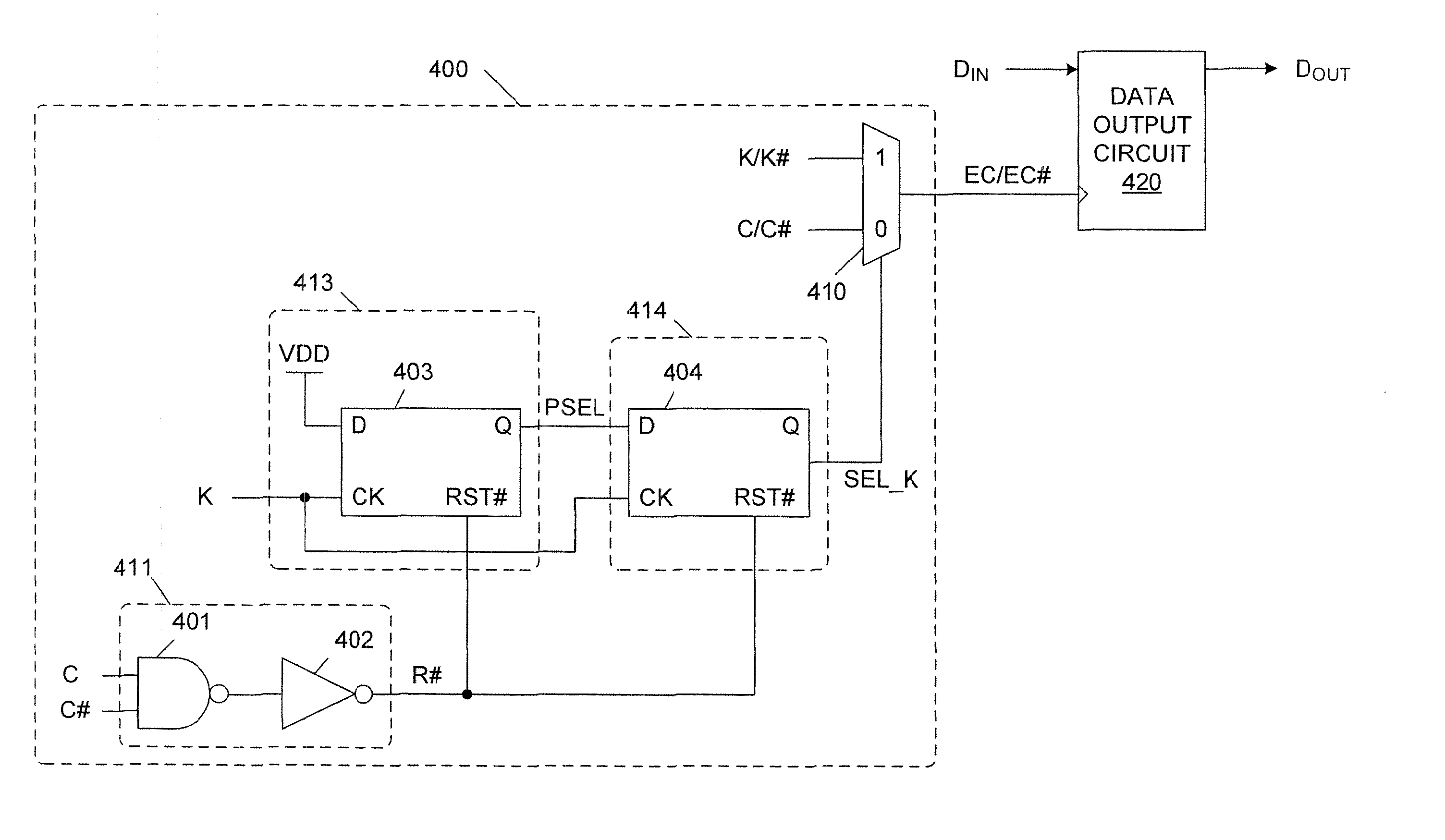
[0025]FIG. 4 is a circuit diagram of a data output clock selection circuit 400 in accordance with one embodiment of the present invention. Data output clock selection circuit 400 includes multiplexer 410, combinational logic circuit 411, and sequential logic circuits 413-414. In the described embodiments, combinational logic circuit 411 is a logical AND circuit formed by logical NAND gate 401 and inverter 402. Sequential logic circuits 413 and 414 are implemented by D-Q flip-flops 403 and 404, respectively, in the described embodiments.
[0026] Logical NAND gate 401 includes a pair of input terminals coupled to receive the output clock signals C and C# (of output clock signal pair C / C#). The output terminal of NAND gate 401 is coupled to an input terminal of inverter 402. Inverter 402 provides a reset control signal R# to the reset input terminals RST# of flip-flops 403 and 404. When the output of inverter 402 has a logic ‘0’ state, flip-flops 403 and 404 are asynchronously reset. Wh...
PUM
 Abstract
Description
Claims
Application Information


