SOI lateral semiconductor device and method of manufacturing the same
- Summary
- Abstract
- Description
- Claims
- Application Information
AI Technical Summary
Benefits of technology
Problems solved by technology
Method used
Image
Examples
first embodiment
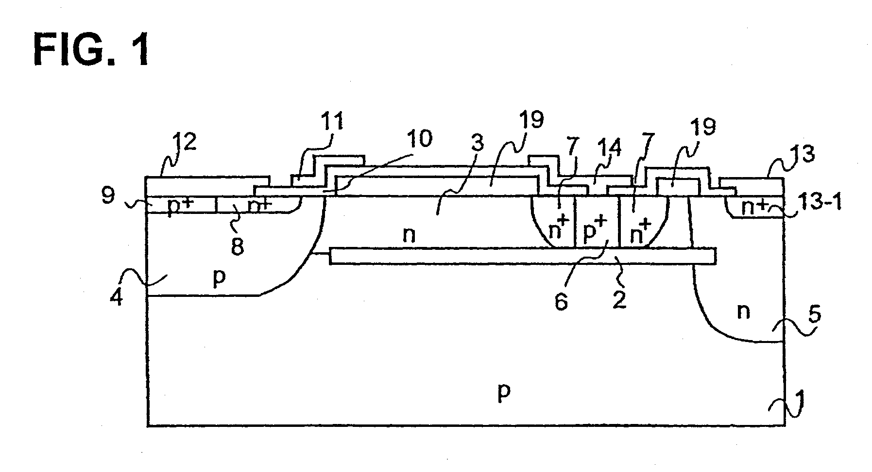
[0036] Referring to FIG. 1, which schematically illustrates a cross-sectional view of a SOI lateral IGBT, the IGBT has a SOI structure comprising a p-type silicon substrate 1, a buried oxide film layer (BOX layer) 2 50 nm thick in the p-type silicon substrate 1, and an n-type silicon active layer 3 around 0.8 μm thick formed on the BOX layer 2 and extending to the semiconductor chip surface. The silicon active layer 3 of n-type provides a very resistive thin film region working as a main current path of the IGBT. In the n-type silicon active layer 3, a p+-type anode region 6 extending from the semiconductor chip surface down to the BOX layer 2 and n+-type buffer regions 7 adjacent to the p+-type anode region 6 are formed.
[0037] At one end region of the BOX layer 2 (nearer the p+-type anode region 6 side of the n-type silicon active layer 3), an n-type well region 5 is formed more deeply than the BOX layer 2. At the opposite end of the n-type silicon active layer 3, a p-type well reg...
fourth embodiment
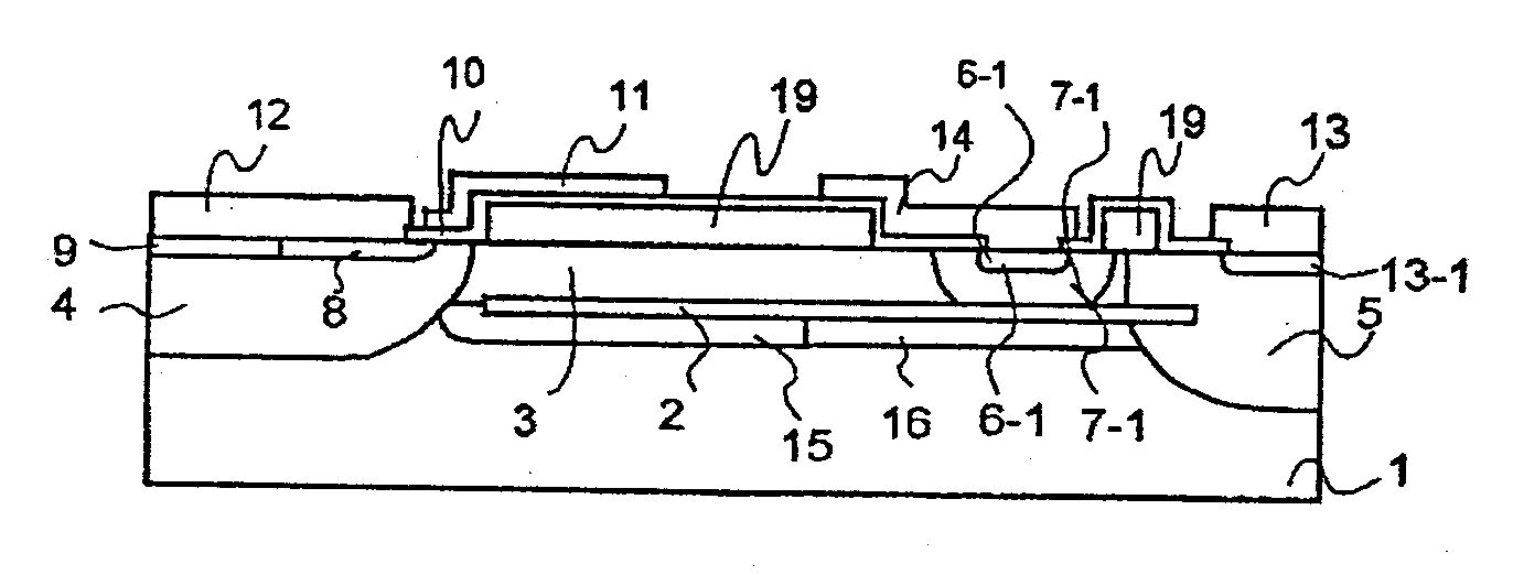
[0061] A LOCOS oxide film 19 of 0.6 μm thick is formed using the nitride mask 38 formed by pattering the nitride film 38. Then, after removing the nitride film, the p+-type anode region 6-1, the n+-type buffer region 7-1, the n+-type emitter region 8, the contact regions 9 and 13-1, the gate electrode 11, the cathode electrode 12, the drain electrode 13, the anode electrode 14, and such constituent elements are formed using a conventional semiconductor process (FIG. 8G), resulting in the lateral IGBT shown in FIG. 7.
[0062]FIG. 9 schematically illustrates a cross-sectional view of a lateral IGBT having a conventional SOI structure. The IGBT shown in FIG. 9 includes a BOX layer 42 formed in the entire major surface of a silicon substrate 41. On the BOX layer 42, an n-type silicon active layer 43 is formed. On one end portion of the n-type silicon active layer 43, an n-type well region (drain region) 45 is formed. On the opposite end portion of the n-type silicon active layer 43, a p-...
sixth embodiment
[0071] The nitride film 87 is patterned to form a nitride mask 87 and the LOCOS oxide film 19 0.6 μm thick is formed. Subsequently, the n+-type emitter region 8, the p+-type anode region 6-1, the n+-type buffer region 7-1, the contact regions 9 and 13-1, the gate electrode 11, the cathode electrode 12, the drain electrode 13, the anode electrode 14, and such constituent elements are formed using a conventional semiconductor process, resulting in the SOI lateral IGBT shown in FIG. 11 (FIG. 15G).
[0072] The sixth embodiment exhibits the simulated ON-losses of 2.78×10⁻⁶ J and the simulated turn-off losses of 1.45×10⁻⁶ J. Therefore, the total losses are 4.23×10⁻⁶ J. The power at the driving frequency 100 kHz is 4.23×10−6×105=0.423 W. The breakdown voltage of the sixth embodiment is 672 V. As compared to the fourth embodiment, the sixth embodiment exhibits almost the same switching losses while improving the breakdown voltage by 12 V.
[0073] The thickness of the BOX layer 2 set at 50 nm ...
PUM
 Abstract
Description
Claims
Application Information


