Semiconductor light emitting device

a technology of semiconductors and light emitting devices, which is applied in semiconductor devices, solid-state devices, lasers, etc., can solve the problems of affecting the heat radiation performance of the light emitting element itself and the metal, generating stress due to the difference in the coefficient of thermal expansion between the light emitting element and the metal as the heat radiating member becomes not negligible, and unable to reduce stress. , to achieve the effect of excellent heat radiation performance and high reliability

Inactive Publication Date: 2007-10-11
SHARP KK
View PDF9 Cites 8 Cited by
  • Summary
  • Abstract
  • Description
  • Claims
  • Application Information

AI Technical Summary

Benefits of technology

[0012]The present invention has been made to solve such problems in conventional technique. An object thereof is to provide a semiconductor light emitting device being excellent in heat radiation performance and highly reliable, which is applicable to a large-size light emitting element, which requires input power of at least 5 W and each edge of which is at least 1 mm.

Problems solved by technology

However, when each edge of the light emitting element exceeds 1 mm, the stress generating due to the difference in coefficient of thermal expansion between the light emitting element itself and the metal as the heat radiating member becomes not negligible.
As a result, the stress cannot be reduced by the brazing material portion and invites the following problems.
That is, peeling of the die-bonding portion may occur, or the light emitting element itself receives the stress and it may deteriorates quickly or be damaged.
Therefore, the stress between the large submount and the metal that is the heat radiating member becomes extremely great.
This also results in peeling of the die-bonding portion or damage between the submount and the metal heat radiating member.
However, because of the great expensiveness and hard workability of these materials, a problem may arise that the light emitting device becomes expensive.
Hence, there has been a problem that, when a large light emitting element is die-bonded to a heat radiating member with a submount interposed, peeling or damage is caused between the submount and the heat radiating member, due to the stress between the members attributed to thermal expansion from the heat.

Method used


Image

  • Semiconductor light emitting device
  • Semiconductor light emitting device
  • Semiconductor light emitting device

Examples


first embodiment

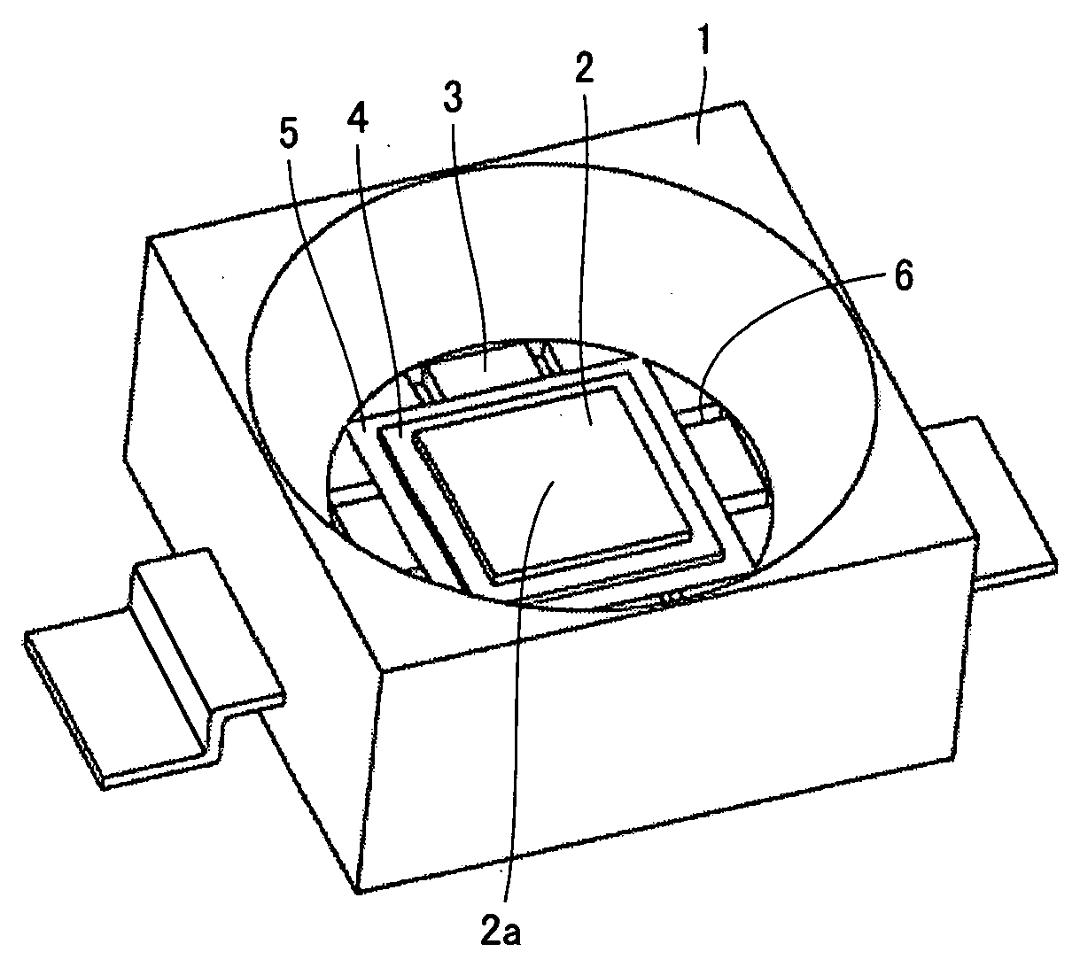
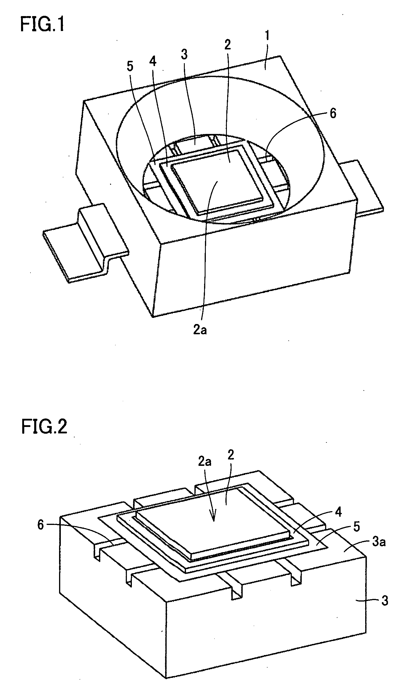
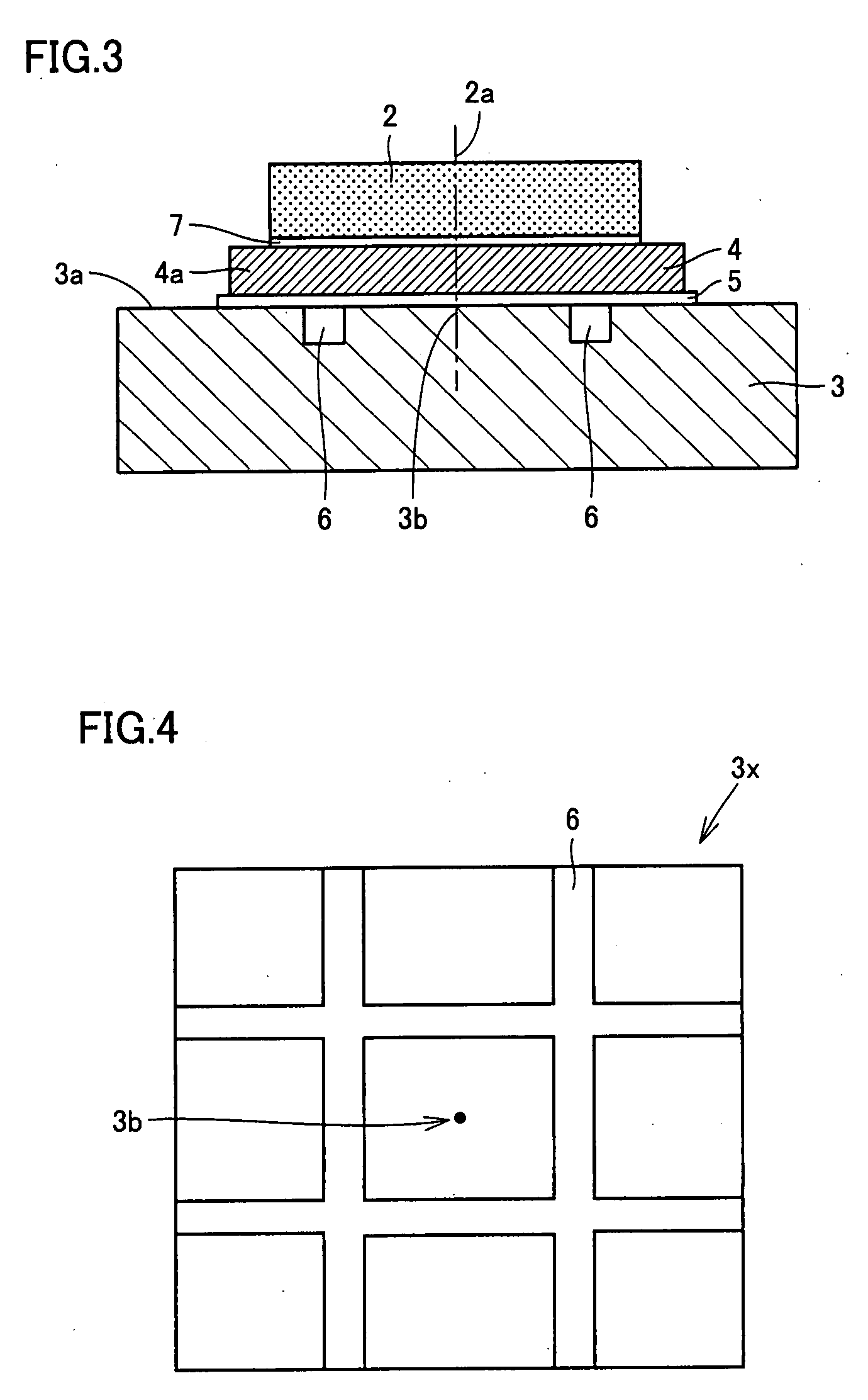
[0025]FIG. 1 is a perspective view showing a semiconductor light emitting device according to a first embodiment of the present invention. FIGS. 2 and 3 are perspective and cross-sectional views, respectively, showing a die-bonded shape of a heat radiating member, a submount, a light emitting element, and a brazing material portion included in the semiconductor light emitting device according to the embodiment of the present invention.

[0026]In the semiconductor light emitting device according to the present embodiment, a light emitting element 2 is fixed to a heat radiating member 3, within a resin package portion 1, by a brazing material 5 with a submount 4 interposed therebetween. On a surface 3a of heat radiating member 3 to which submount 4 is fixed, a groove 6 is formed. That is, on surface 3a of heat radiating member 3 on the die-bond side, groove 6 is formed. Submount 4 is die-bonded on surface 3a, using brazing material 5 such as solder or silver paste. On submount 4, light ...

second embodiment

[0030]Next, a second embodiment of the present invention will be described. Groove 6 can be arranged with considerably great degree of freedom, so long as it is not formed immediately below the heat radiating portion or immediately below the center of the light emitting element. Accordingly, in the second embodiment of the present invention, as shown in FIG. 4, at the surface of heat radiating member 3x, groove 6 is formed as lines perpendicularly crossing each other at right angles, so as to surround a rectangular plane region that includes portion 3b immediately below the center of light emitting element 2.

[0031]In the plan region occupied by light emitting element 2, it is desirable that the region surrounded by groove 6 is divided to be about 1 mm2 at most. If brazing materials 5 and 7 rise along light emitting element 2 or submount 4 and adhere to the sides, interfacial debonding or crack is likely to occur. Therefore, the amount of brazing materials 5 and 7 must be appropriate...

third embodiment

[0032]Next, a third embodiment of the present invention will be described in the following. In the third embodiment, as shown in FIG. 5, groove 6 is formed not at a plan region of heat radiating member 3y and portion 3b immediately below the center of light emitting element 2, but to surround a circular plan region that includes portion 3b immediately below the center of light emitting element 2. In the present embodiment also, groove 6 is formed on the die-bond surface so that brazing material 5 does not rise along light emitting element 2 or submount 4 and adhere to the sides. Therefore, redundant brazing material 5 accumulates in groove 6 and the rise thereof can be prevented.

[0033]As described above, in any of the embodiments, basically heat radiating member 3, 3x and 3y below submount 4 region is divided by groove 6. Thus, the stress due to the difference in thermal expansion between each member is reduced. It should be noted that it is often the peripheral portion of submount ...


PUM


Abstract

A semiconductor light emitting device includes a light emitting element, a heat radiating member, and a submount interposed between the light emitting element and the heat radiating member. The light emitting element is fixed to heat radiating member by a brazing material with the submount interposed. The heat radiating member has a groove on its surface to which the submount is fixed. With this configuration, a semiconductor light emitting device that is applicable to a large-sized light emitting element that is excellent in heat radiation and that has high reliability can be provided.

Description

[0001]This nonprovisional application is based on Japanese Patent Application No. 2006-104481 filed with the Japan Patent Office on Apr. 5, 2006, the entire contents of which are hereby incorporated by reference.BACKGROUND OF THE INVENTION[0002]1. Field of the Invention[0003]The present invention relates to a semiconductor light emitting device, which is used in an illumination apparatus, a light source of a projector or the like that employs a light emitting element that primarily uses white light.[0004]2. Description of the Background Art[0005]A semiconductor light emitting device of the high output type that includes a large-size light emitting element, which consumes great power, requires input power of at least 5 W, and each edge of which is at least 1 mm, requires measures for heat radiation. As the measures for heat radiation, conventionally, a structure shown in FIG. 6 has generally been employed. Specifically, it is a structure in which a light emitting element 100 is fixed...

Claims


Application Information

Patent Timeline
Patent Type & Authority Applications(United States)
IPC IPC(8): H01S3/04H01L33/62H01L33/64
CPCH01L33/64H01L33/642H01L2924/0002H01L2924/00
Inventor CHIKUGAWA, HIROSHI
Owner SHARP KK
Why Eureka
Try Eureka