Magnetic sensor, production method of the same, and target substance detecting apparatus and biosensor kit using the same
a technology of magnetometer and target substance, which is applied in the direction of analytical tools using chemical indicators, laboratory glassware, instruments, etc., can solve the problems of requiring a large measuring apparatus, and unable to detect the number or concentration of antigens
- Summary
- Abstract
- Description
- Claims
- Application Information
AI Technical Summary
Benefits of technology
Problems solved by technology
Method used
Image
Examples
example 1
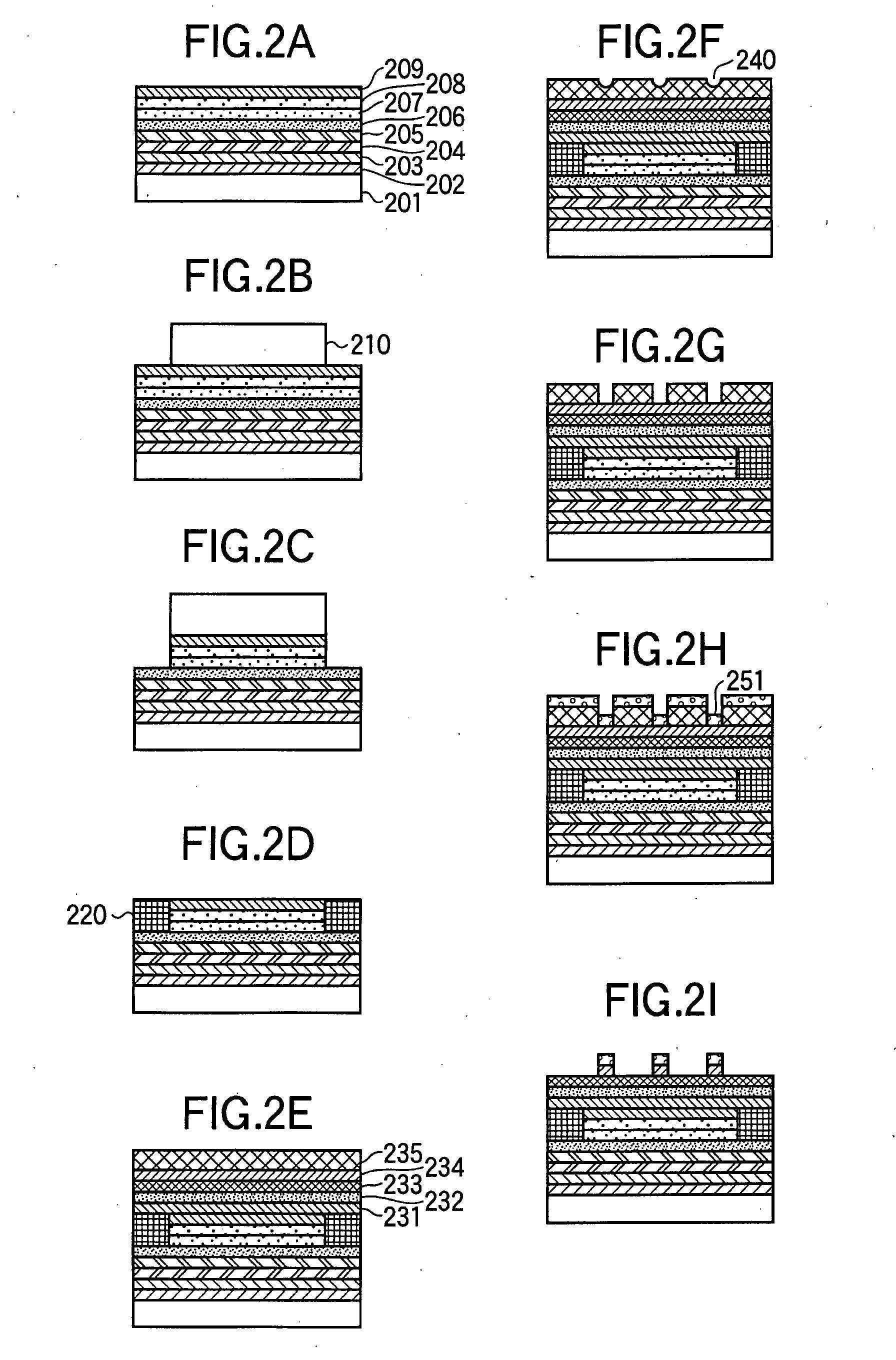
[0071]In this example, an example of a production method of a magnetic sensor according to the present invention will be described with FIGS. 2A to 2I.
[0072]On a surface of a silicon wafer 201, a multilayer structure is obtained by sequentially stacking a Cr film 202 at 20 nm film thickness, a Pt film 203 at 20 nm film thickness, an MnIr film 204 at 10 nm film thickness, an FeCo film 205 at 5 nm film thickness, an Al2O3 film 206 at 1.6 nm film thickness, an FeCo film 207 at 5 nm film thickness, an NiFe film 208 at 20 nm film thickness, and a Pt film 209 at 5 nm film thickness by magnetron sputtering (FIG. 2A). As for the Al2O3 film 206, oxygen deficiency is compensated by forming a film using an Al2O3 target, introducing an O2 gas in a film formation chamber, and performing plasma oxidation. Starting from a silicon wafer 201 side, the Cr / Pt multilayer film becomes a base electrode of a TMR element, the Mnlr / FeCo multilayer film becomes a pin layer (layer whose magnetizing direction ...
example 2
[0094]Although the production method of the Au dot pattern using anodic oxidation was described in the first example, Au dots can be also formed into a desired pattern using an Au target which has a needle-shaped section.
[0095]An SiN film 233 at 30 nm film thickness is formed on a surface of the multilayer film structure in the state that the magnetic sensor of FIG. 2D in the first example is formed. Then, a resist film is coated at about 1-μm uniform film thickness by a spin coater. Subsequently, patterning is performed with ultraviolet rays after baking, for example, so that a resist film may cover an area where Au dots are not formed, such as an area other than an area above the sensor element. Then, the multilayer film structure is baked again, and is immersed in a developing solution to be cleaned with deionized water, and then, a resist film with a desired pattern shape is obtained. Next, an acicular Au target and a treated surface are arranged with making the acicular Au targ...
example 3
[0098]Furthermore, by forming micropores in an upper portion of the element by resist film patterning, and forming Au films on the pores, Au dots can be also formed into a desired pattern.
[0099]An SiN film 233 at 30 nm film thickness is formed on a surface of the multilayer film structure in the state that the magnetic sensor of FIG. 2D in the first example is formed. Then, a resist film is coated at about 200 nm uniform film thickness by a spin coater. After baking, holes are formed by radiating electron rays in positions where Au dots are formed. Then, the multilayer film structure is baked again, and is immersed in a developing solution to be cleaned with deionized water, and then, a resist film with a desired pattern shape is obtained. Diameter of the holes formed is about φ50 nm diameter, and the interval between adjacent holes is made larger than the grain size of labeling substances. Subsequently, an Au film is formed in each hole by a low directive film formation apparatus, ...
PUM
 Abstract
Description
Claims
Application Information
 - R&D
- Intellectual Property
- Life Sciences
- Materials
- Tech Scout
- Unparalleled Data Quality
- Higher Quality Content
- 60% Fewer Hallucinations
Browse by: Latest US Patents, China's latest patents, Technical Efficacy Thesaurus, Application Domain, Technology Topic, Popular Technical Reports.
© 2025 PatSnap. All rights reserved.Legal|Privacy policy|Modern Slavery Act Transparency Statement|Sitemap|About US| Contact US: help@patsnap.com


