Processing apparatus

a processing apparatus and processing technology, applied in the direction of solid-state devices, instruments, semiconductor/solid-state device details, etc., can solve the problems of increased cost, reduced cost, and not necessarily optimal edram-based design

Active Publication Date: 2007-10-11
SONY COMPUTER ENTERTAINMENT INC
View PDF5 Cites 15 Cited by
  • Summary
  • Abstract
  • Description
  • Claims
  • Application Information

AI Technical Summary

Benefits of technology

[0009] The present invention has been developed in view of the foregoing challenges, and a general purpose thereof is to provide a processing apparatus which has processing power that is well balanced with cost.
[0011] According to this embodiment, the plurality of processors is provided with respective memory controllers and memories individually, instead of a single memory being shared among the processors. This makes it possible to apply memory management that is optimal for each individual processor. Moreover, since the plurality of processors and the plurality of memories are integrated on separate semiconductor substrates, it is possible to select an optimal process for forming processors, or logic, and an optimal process for forming memories such as a DRAM.
[0013] In this embodiment, the plurality of processors and the respective plurality of memories are individually connected to each other. The micro-bump connection makes it possible to design in bit width without limitations, and can reduce the area occupied by a semiconductor chip.
[0015] According to this embodiment, a bus between the arithmetic processor and the application-specific processors that are integrated on the first semiconductor substrate can be built into the semiconductor substrate. This makes stable signal processing possible. The image processor and the memory to be managed by the image processor often have to be connected to each other with a broad bandwidth. Therefore, the image processor and the memory may be designed as separate chips outside the first and second semiconductor substrates. This allows for a throughput-oriented design.
[0018] According to this embodiment, a manufacturing process optimal for designing processors, i.e., designing logic circuits can be selected as the manufacturing process of the first semiconductor substrate, and a manufacturing process optimal for designing memory arrays can be selected as the manufacturing process of the second semiconductor substrate. This can guarantee the effect of improved yield, reduced area of occupation, and any associated cost reduction.
[0020] According to this embodiment, the processors and the memories are classified by optimal manufacturing processes in consideration of throughput, cost, power consumption, and the like required of the respective components. This makes it possible to optimize the design of the entire processing apparatus.

Problems solved by technology

Under the circumstances, it has been a significant challenge to achieve cost reduction while integrating the processors and the memories needed to satisfy performance requirements.
When the most advanced processes are used, the incorporation of DRAMs, which do not require integration to a level as high as the processors, can result in increased cost.
In such situations, the eDRAM-based design is not necessarily optimal.
Under the circumstances, for arithmetic processing apparatuses that incorporate a high-performance graphics processor and the like for handling three-dimensional graphics, it is a significant challenge to optimize the balance between performance and cost with respect to how to integrate a CPU which performs general-purpose arithmetic processing and application-specific processors which are dedicated and designed for specific processing such as graphics and input and output signal processing.

Method used


Image

  • Processing apparatus
  • Processing apparatus
  • Processing apparatus

Examples


first configuration example

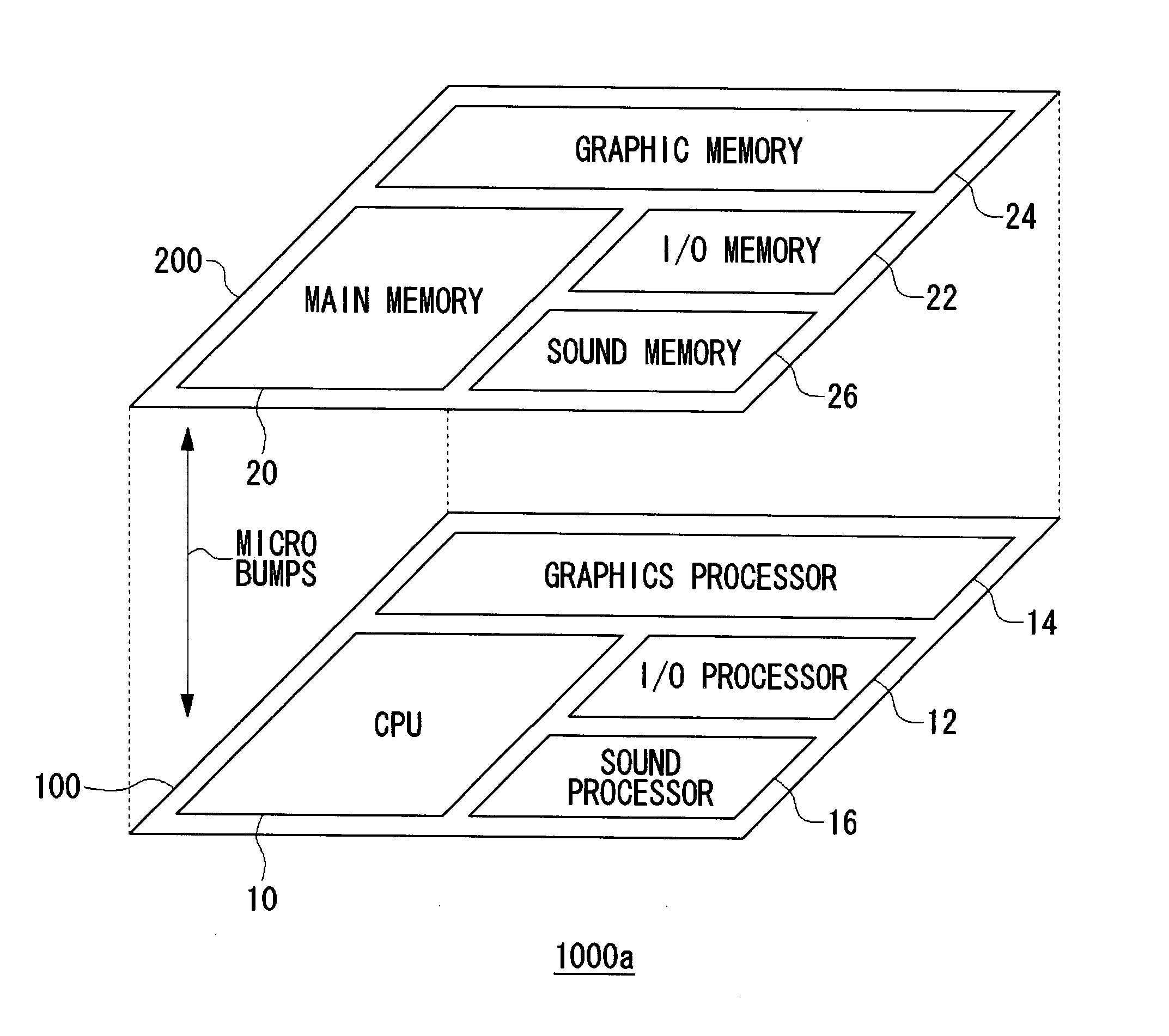
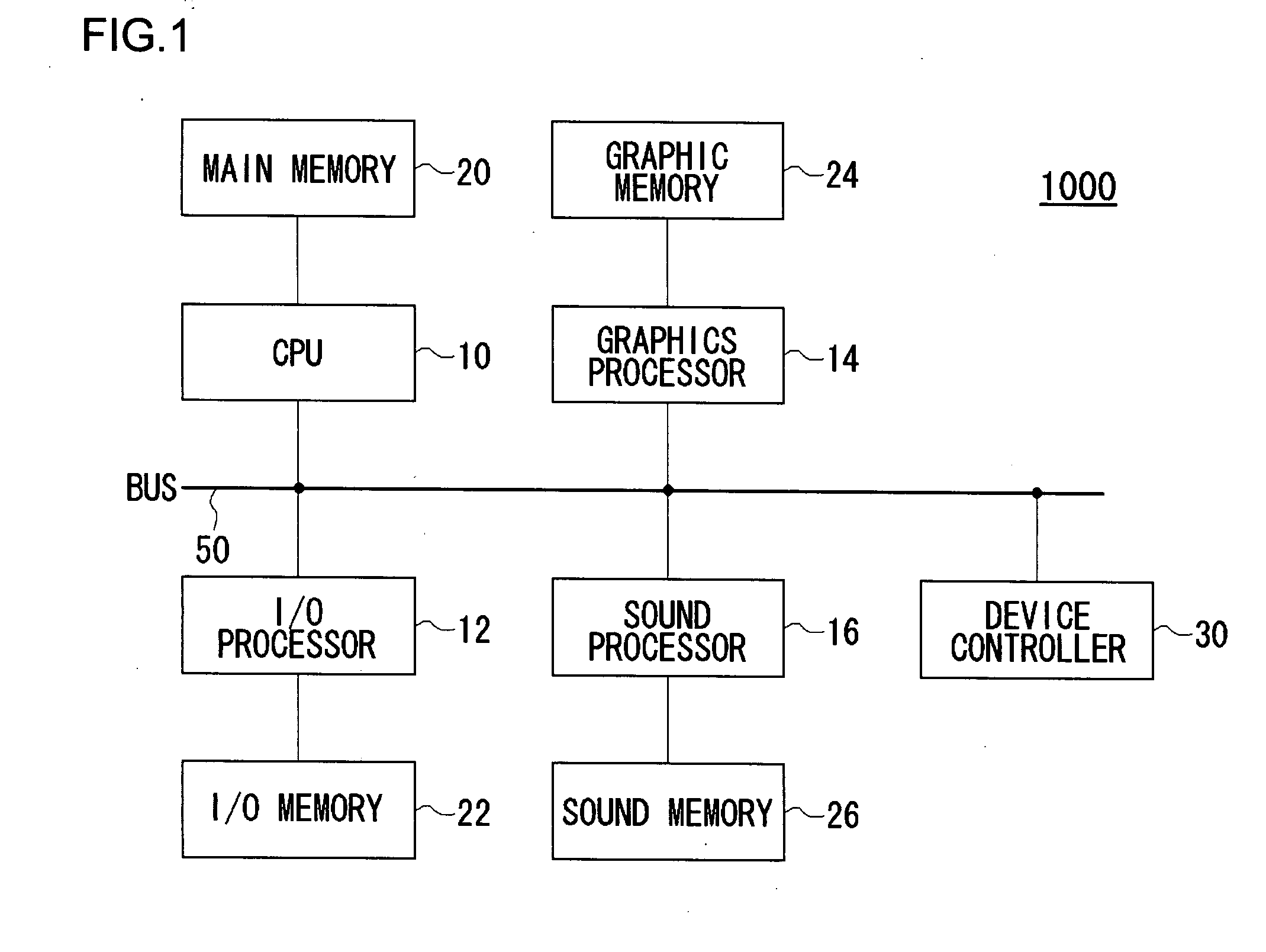
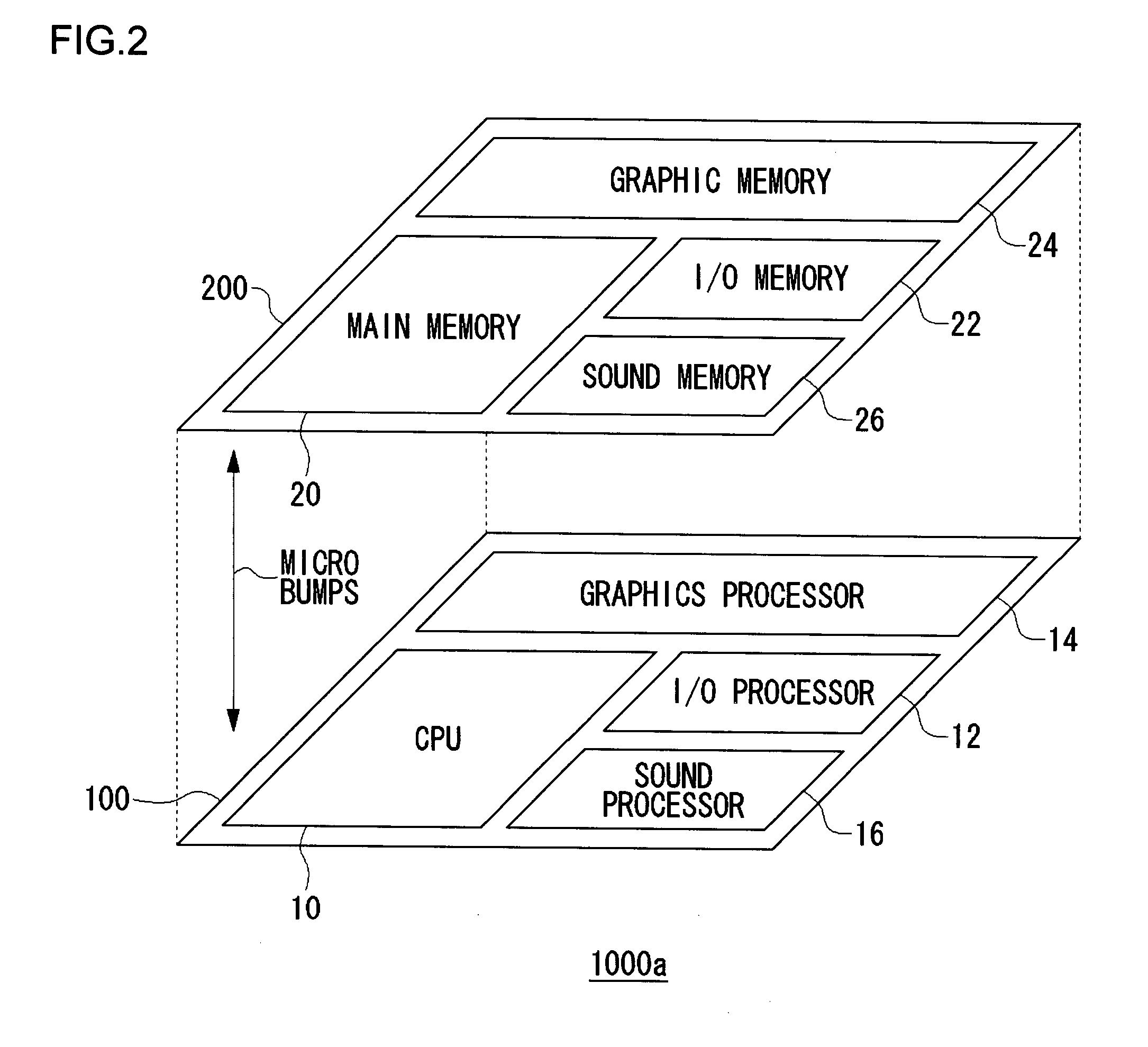
[0039] In a first configuration example, the CPU 10, the I / O processor 12, the graphics processor 14, and the sound processor 16 are integrated on one semiconductor substrate. The main memory 20, the I / O memory 22, the graphic memory 24, and the sound memory 26 are integrated on another semiconductor substrate. FIG. 2 is a diagram showing the configuration of an arithmetic processing apparatus 1000a according to the first configuration example. The arithmetic processing apparatus 1000a includes a first semiconductor substrate 100 and a second semiconductor substrate 200. The CPU 10, the I / O processor 12, the graphics processor 14, and the sound processor 16 are integrated on the first semiconductor substrate 100. The main memory 20, the I / O memory 22, the graphic memory 24, and the sound memory 26 are integrated on the second semiconductor substrate 200. The device controller 30 and the like may also be integrated on the first semiconductor substrate 100. In fact, the first semicond...

second configuration example

[0046]FIG. 3 is a diagram showing the configuration of an arithmetic processing apparatus 1000b according to a second configuration example. Hereinafter, a description will be given of the differences between the first configuration example and the second configuration example. In the arithmetic processing apparatus 1000b of FIG. 3, the graphics processor 14 and the graphic memory 24 are not integrated on the first semiconductor substrate 100 and the second semiconductor substrate 200, respectively. That is, what are integrated on the first semiconductor substrate 100 are the CPU 10, and the I / O processor 12 and the sound processor 16 that are the application-specific processors excluding the graphics processor 14 which performs image processing. What are integrated on the second semiconductor substrate 200 are the main memory 20 to be managed by the CPU 10, and the application-specific memories to be managed by the application-specific processors other than the graphics processor 1...

third configuration example

[0051] The first configuration example translates into an example where the first semiconductor substrate 100 and the second semiconductor substrate200 are configured separately in view of the circuit functions of processors and memories. In the third configuration example, the individual elements of FIG. 1, i.e., the plurality of processors and the plurality of memories to be managed by the plurality of processors are classified depending on the semiconductor manufacturing processes optimal for manufacturing the respective circuit blocks, regardless of the functions thereof. Then, the components classified into an identical semiconductor manufacturing process are formed on the same semiconductor substrate. The “optimal processes” refer to processes that are determined in a comprehensive manner, for example, based on the throughput, cost, power consumption, and the like required of each component.

[0052] Following the design concept of the third configuration example may also result...


PUM


Abstract

In a processing apparatus, a plurality of processors which perform different kinds of processing is integrated on a first semiconductor substrate. A plurality of memories to be managed by the plurality of processors integrated on the first semiconductor substrate is integrated on a second semiconductor substrate. The plurality of processors integrated on the first semiconductor substrate includes respective separate memory controllers which control the memories to be managed that are integrated on the second semiconductor substrate. The semiconductor substrates are manufactured using different semiconductor manufacturing processes, and micro bumps are formed on their respective surfaces. The semiconductor substrates are stacked together in the thickness direction, and are connected to each other through the micro bumps.

Description

BACKGROUND OF THE INVENTION [0001] 1. Field of the Invention [0002] The present invention relates to a processing apparatus, and in particular, to a processing apparatus which has processors for performing a plurality of different kinds of processing. [0003] 2. Description of the Related Art [0004] Personal computers, workstations, and high-performance game consoles have been advancing in functionality and performance in recent years. Arithmetic processing apparatuses to be used therein have therefore been increasing in circuit scale. These arithmetic processing apparatuses typically comprise a CPU (Central Processing Unit) or other processors which perform general-purpose arithmetic processing, a processor which manages signal input and output, a processor which performs audio signal processing, and a graphics processor which performs image processing, as well as memories to be used and managed by the processors. [0005] Under the circumstances, it has been a significant challenge t...

Claims


Application Information

Patent Timeline
Patent Type & Authority Applications(United States)
IPC IPC(8): G06F17/50H01L23/02
CPCH01L25/0657H01L25/18H01L2225/06513H01L2924/0002H01L2924/00
Inventor HIROI, TOSHIYUKISUGAWARA, AKIHIKO
Owner SONY COMPUTER ENTERTAINMENT INC
Why Eureka
Try Eureka