Electronic Part and Manufacturing Method Thereof

a manufacturing method and technology for electronic parts, applied in the field of electronic parts, can solve the problems of reducing the electric characteristics of filters, affecting the selection of piezoelectric/electrostrictive devices, and unable to obtain adequate attenuation values on the reception side, and achieve the effect of superior temperature coefficient and electric characteristics

Active Publication Date: 2007-10-18
SKYWORKS PANASONIC FILTER SOLUTIONS JAPAN
View PDF5 Cites 15 Cited by
  • Summary
  • Abstract
  • Description
  • Claims
  • Application Information

AI Technical Summary

Benefits of technology

[0010] In order to solve the above described conventional disadvantages, it is an object of the present invention to provide an electronic part having superior temperature coefficient and electric characteristics by forming a protective film on an electrode.

Problems solved by technology

However, depending on a place at which a filter is used in a mobile phone system or its radio circuit section, filter characteristics are required, such as a small insertion loss within a further passing band and a steep skirt property of the filter, as well as a high suppression level within a block band.
This is disadvantageous in temperature coefficient.
Thus, for example, if the transmission band is desired to be secured over the entire temperature (i.e., within the whole range of ±50° C. at the room temperature), an adequate attenuation value cannot be obtained on the reception side.
Accordingly, unwanted reflection occurs at edges of concave portions of the insulating film, which may degrade electric characteristics of the filter.

Method used


Image

  • Electronic Part and Manufacturing Method Thereof
  • Electronic Part and Manufacturing Method Thereof
  • Electronic Part and Manufacturing Method Thereof

Examples


first embodiment

[0024] In this section, the invention is described by way of the first embodiment.

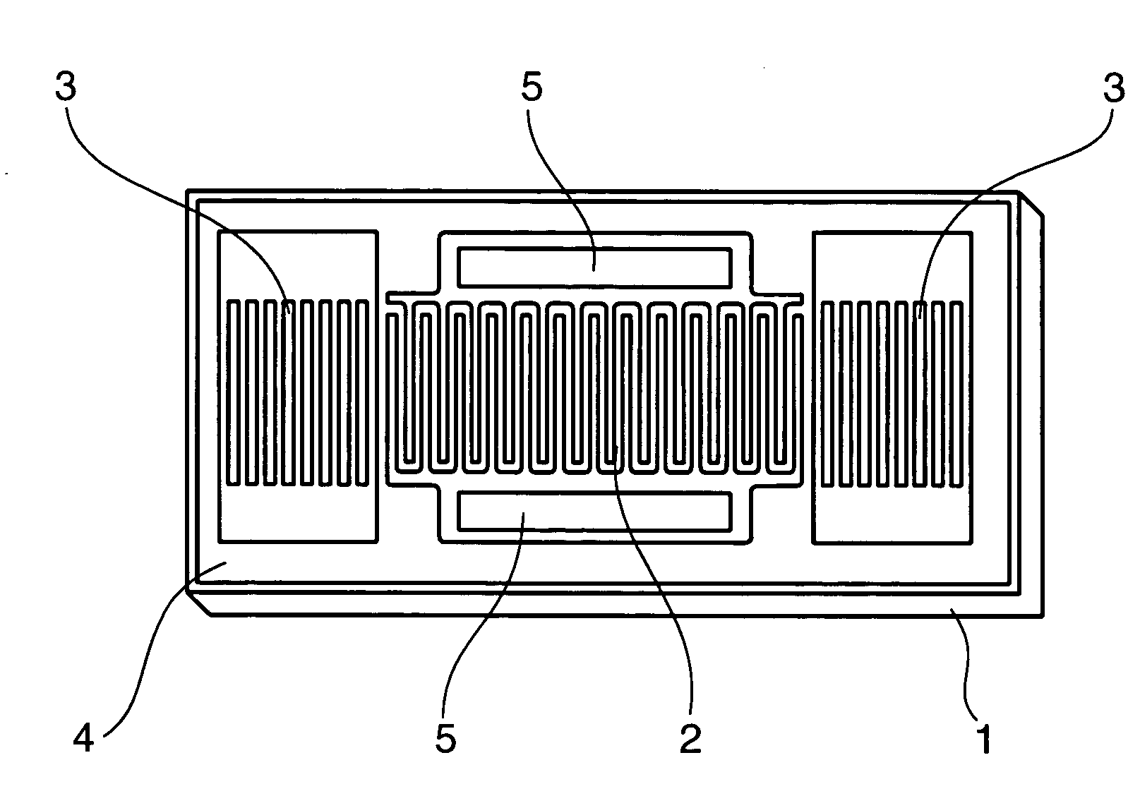
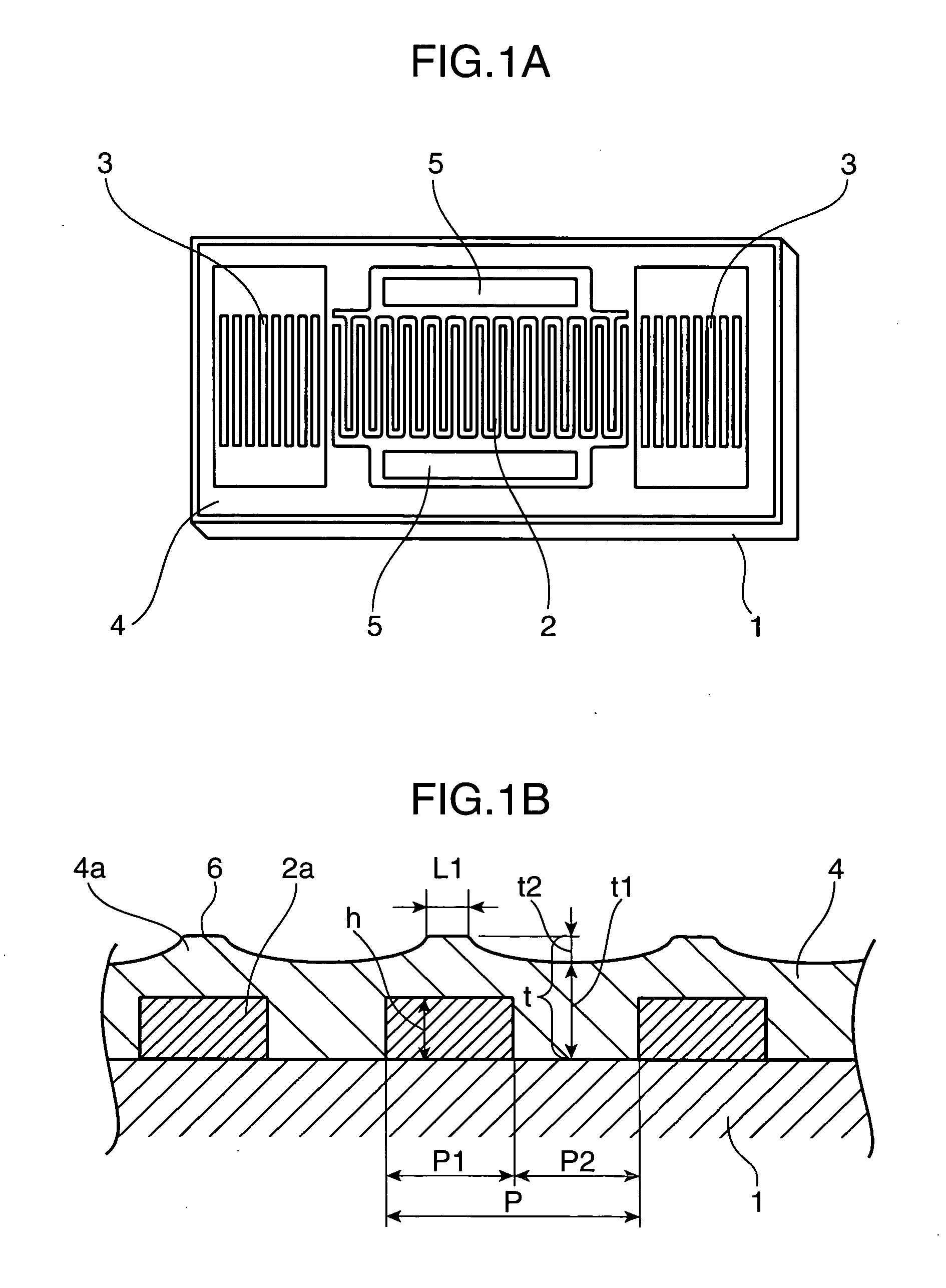
[0025]FIG. 1A is a top plan view of an SAW device, as the electronic part in the first embodiment of the invention, and FIG. 1B is a cross-sectional view of FIG. 1A.

[0026] As shown in FIGS. 1A and 1B, the SAW device in the first embodiment includes: a comb-shaped electrode 2 having a plurality of electrode fingers 2a arranged parallel to one another on the upper surface of a substrate 1; reflective electrodes 3 disposed on both sides of the comb-shaped electrode 2 in the arranged direction of the electrode fingers 2a; and a protective film 4 for covering at least the comb-shaped electrode 2 and the reflective electrodes 3. A pad 5 is electrically connected to the comb-shaped electrode 2 to take an electric signal out of the comb-shaped electrode 2.

[0027] The substrate 1 is a lithium tantalate (hereinafter, called as “LT”) substrate which is cut of a Y-axis at a certain rotational angle around the X-...

second embodiment

[0062] In this section, an SAW device in the second embodiment of the invention is described referring to the drawings.

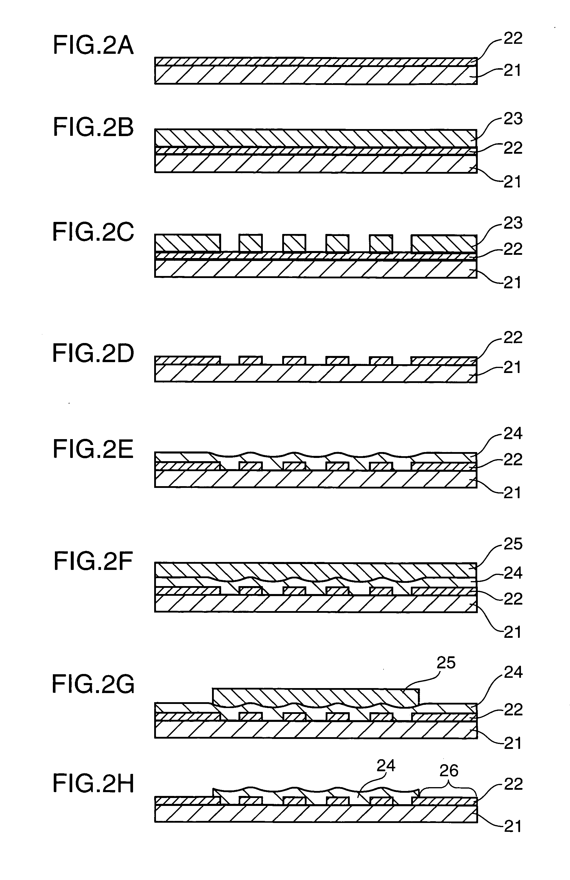
[0063] In the second embodiment, an SAW device substantially identical to the SAW device in the first embodiment is used. The method for manufacturing the SAW device in the second embodiment is substantially equivalent to the method described in the first embodiment except for the following. Specifically, a so-called bias sputtering method of forming a film by sputtering, with a bias voltage being applied on the substrate side in forming an SiO2 film, as illustrated in FIG. 2E, is used in a method for manufacturing an SAW device comprising a substrate; a comb-shaped electrode formed on the upper surface of the substrate; and a protective film which covers the comb-shaped electrode, and has convex portions and concave portions on an upper surface thereof, wherein an uppermost surface of the protective film has, in cross section in a direction orthogonal to an extend...


PUM

PropertyMeasurementUnit
rotational angleaaaaaaaaaa
temperatureaaaaaaaaaa

Abstract

An electronic part includes: a substrate; a comb-shaped electrode having a plurality of electrode fingers arranged parallel to one another on the upper surface of the substrate; and a protective film formed on the upper surface of the substrate so as to cover the comb-shaped electrode. The protective film has convex portions and concave portions. The convex portions are upwardly convex at the positions corresponding to the electrode fingers, and the concave portions are downwardly concave between the convex portions. The cross section of the protective film in the direction orthogonal to the extending direction of the electrode fingers has a downward convex curve between apex portions of the convex portions.

Description

TECHNICAL FIELD [0001] The present invention relates to an electronic part such as a surface acoustic wave device, and a manufacturing method thereof. BACKGROUND ART [0002] Hereinafter, a conventional electronic part will be described. [0003] In the prior art, a surface acoustic wave device (hereinafter, called as “SAW device”) is described as an example of an electronic part. [0004] In recent years, a compact and lightweight SAW device is prevalently used for electronic equipment such as various types of mobile communication terminal equipment. In particular, in a radio circuit section of a mobile phone system within a band of 800 MHz to 2 GHz, an SAW filter has been widely used. Such an SAW filter is formed by a lithium tantalate (hereinafter, called as “LT”) substrate which is cut of a Y-axis at a cut angle of 36° as its rotational angle around the X-axis in the Z-axis direction, or a so-called 36° Y-cut X-propagation LT (hereinafter, called as “36° YLT”) substrate. However, depe...

Claims


Application Information

Patent Timeline
Patent Type & Authority Applications(United States)
IPC IPC(8): H03H9/145H01L41/09H01L41/18H01L41/23H03H3/08
CPCY10T29/49002H03H3/10H03H9/145
Inventor TAKAYAMA, RYOUICHIIWASAKI, YUKIO
Owner SKYWORKS PANASONIC FILTER SOLUTIONS JAPAN
Why Eureka
Try Eureka