Device to protect semiconductor device from electrostatic discharge

Inactive Publication Date: 2007-10-18
SK HYNIX INC
View PDF5 Cites 5 Cited by
  • Summary
  • Abstract
  • Description
  • Claims
  • Application Information

AI Technical Summary

Benefits of technology

[0026]The present invention provides a device to protect a semiconductor device from electrostatic discharge (ESD), which can safely protect an internal circuit from static electricity by performing smoothly a discharging operation with minute current in a latter part of the static electricity.

Problems solved by technology

Generally, electrostatic discharge (ESD) is one of the important factors that can adversely influence the reliability of a semiconductor device.
Because of this, a junction, a contact, a gate oxide film or other components located inside of the semiconductor device are melted, thereby resulting in failure.
Particularly, the thickness of the gate insulation film of a transistor consisting of an input / output buffer is more reduced with the development of manufacturing technology of semiconductor devices and thus an internal circuit can be more easily damaged.
However, the voltage drop generated in the detecting unit 12 is limited to the alternating current in the rising section of the static electricity and therefore the time in which the detection voltage is detected is short.
In other words, since the operational duration of the device is short, it is difficult to protect the internal circuit 16 from the static electricity.
As a result, the internal circuit 16 may be damaged in sections due to the relatively rapide rise and fall of the static electricity.
In this case, the operation of the device is not sufficient and may damage the internal circuit 26 of the semiconductor device during a later part of the pulse in which the static electricity becomes small.

Method used


Image

  • Device to protect semiconductor device from electrostatic discharge
  • Device to protect semiconductor device from electrostatic discharge
  • Device to protect semiconductor device from electrostatic discharge

Examples


first embodiment

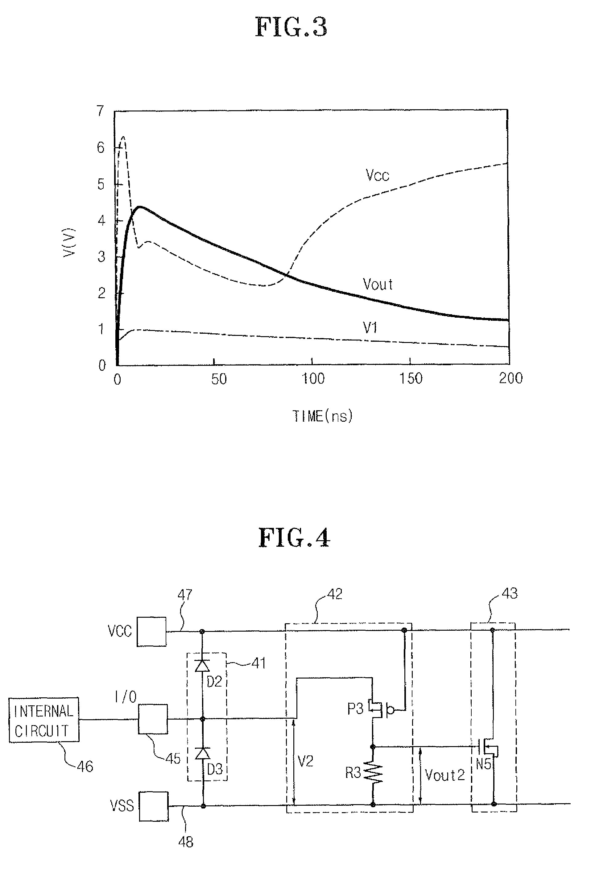
[0063]FIG. 4 is a circuit diagram illustrating a device for use in protecting a semiconductor device from ESD damage according to the present invention.

[0064]The device to protect a semiconductor device from ESD according to a first embodiment of the present invention is provided with a transferring unit 41, a detecting unit 42 and a discharging unit 43.

[0065]The transferring unit 41 includes diodes D2 and D3, which are serially connected between an external voltage line 47 and a grounding voltage line 48. A cathode of the diode D2 is connected to the external voltage line 47 and an anode of the diode D3 is connected to the grounding voltage line 48. The transferring unit 41 transfers static electricity to the external voltage line 47 so that the static electricity inputted from the input / output terminal 45 is not transferred to an internal circuit.

[0066]The detecting unit 42 includes a PMOS transistor P3 and a resistance element R3, which are serially connected between the input / ou...

second embodiment

[0077]The device to protect a semiconductor device from ESD according to the present invention shown in FIG. 6 is adapted to protect an internal circuit 66 from negative (−) static electricity inputted to the input / output terminal 65 in a case in which the elements in the internal circuit 66 connected to the external voltage line 67 are very weak.

[0078]In FIG. 6 a PMOS transistor P4 is provided as a discharging unit 63 unlike the first embodiment in which a NMOS transistor N5 is provided as the discharging unit 43, as shown in FIG. 4. Further, the detecting unit 62 includes a resistance element R4 and a NMOS transistor N6, which are serially connected between the external voltage line 67 and a grounding voltage line 68. Here, the gate of the NMOS transistor N6 is connected to the grounding voltage line 68, the drain to the input / output terminal and the source to the resistance element R4.

[0079]Referring to the operation of the device to protect a semiconductor from an ESD according ...

third embodiment

[0081]The device for use in protecting a semiconductor device from ESD according to the present invention shown in FIG. 7 is further provided with an amplifying unit 74 between the detecting unit 72 and the discharging unit 73 to enhance the driving ability of the discharging unit 73.

[0082]The amplifying unit 74 includes two CMOS type inverters having a PMOS transistor and a NMOS transistor, which are serially connected between the external voltage line 77 and the grounding voltage line 78.

[0083]Discharging operation can be performed more stably as the detection voltage detected in the detecting unit 72 is sufficiently amplified by the amplifying unit 74 and then applied to the discharging unit 73. Thus, the device to protect a semiconductor device from ESD protects the internal circuit 76 of the semiconductor device from the static electricity inputted to the input / output terminal 75.


PUM


Abstract

A device to protect a semiconductor device from electrostatic discharge includes a transferring unit transferring the static electricity inputted to said input / output terminal to the power line, a detecting unit sensing the potential difference between both ends of the transferring unit, located between an input / output terminal and one of the power lines, to output the detection voltage, and a discharging unit driven by said detection voltage and discharging the static electricity led to a specific power line to the other power line, and performs the discharging operation smoothly even with minute electrostatic current and a latter part of the static electricity by using the driving voltage, which is used to drive a conventional detecting unit, as the driving voltage of the ESD protection device, thereby safely protecting an internal circuit of a semiconductor device.

Description

CROSS-REFERENCE TO RELATED APPLICATIONS[0001]The present application claims priority to Korean patent application number 10-2006-0035015 filed on Apr. 18, 2007, which is incorporated herein by reference in its entirety.BACKGROUND OF THE INVENTION[0002]The present invention relates to a device to protect a semiconductor device from electrostatic discharge (ESD), and more particularly, to a device that protects the semiconductor device from ESD and resulting damage from the ESD.[0003]Generally, electrostatic discharge (ESD) is one of the important factors that can adversely influence the reliability of a semiconductor device. Such electrostatic phenomenon can be classified into a human body model (HBM), a machine model (MM) and a charge device model (CDM) according to causes of the occurrence of the static electricity. The HBM is an electrostatic phenomenon resulting from a human body, the MM is an electrostatic phenomenon resulting from contact with a measuring machine and the CDM is...

Claims


Application Information

Patent Timeline
IPC IPC(8): H02H9/00
CPCH02H9/046H01L27/04
Inventor CHOI, NAK HEON
Owner SK HYNIX INC
Why Eureka
Try Eureka