Through Substrate, Interposer and Manufacturing Method of Through Substrate

Inactive Publication Date: 2007-10-25
TOKYO ELECTRON LTD
View PDF15 Cites 11 Cited by
  • Summary
  • Abstract
  • Description
  • Claims
  • Application Information

AI Technical Summary

Benefits of technology

[0025] As a result, the interposer can be provid

Problems solved by technology

A conventional multilayer wiring circuit substrate has a problem in that a crosstalk noise is generated in signal wirings because signal lines are close to each other due to high density of wiring layers, and an operation defect is generated in a driving element of the circuit.
However, there is a problem in

Method used


Image

  • Through Substrate, Interposer and Manufacturing Method of Through Substrate
  • Through Substrate, Interposer and Manufacturing Method of Through Substrate
  • Through Substrate, Interposer and Manufacturing Method of Through Substrate

Examples


Example

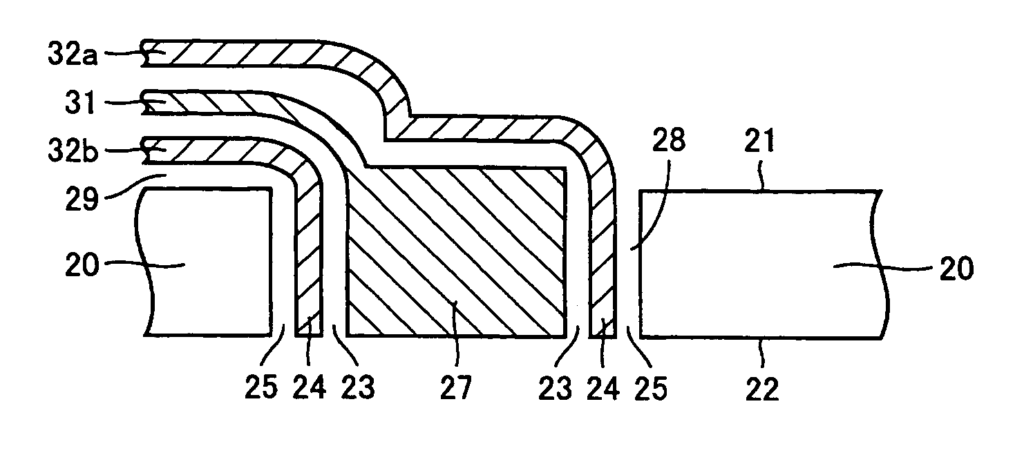
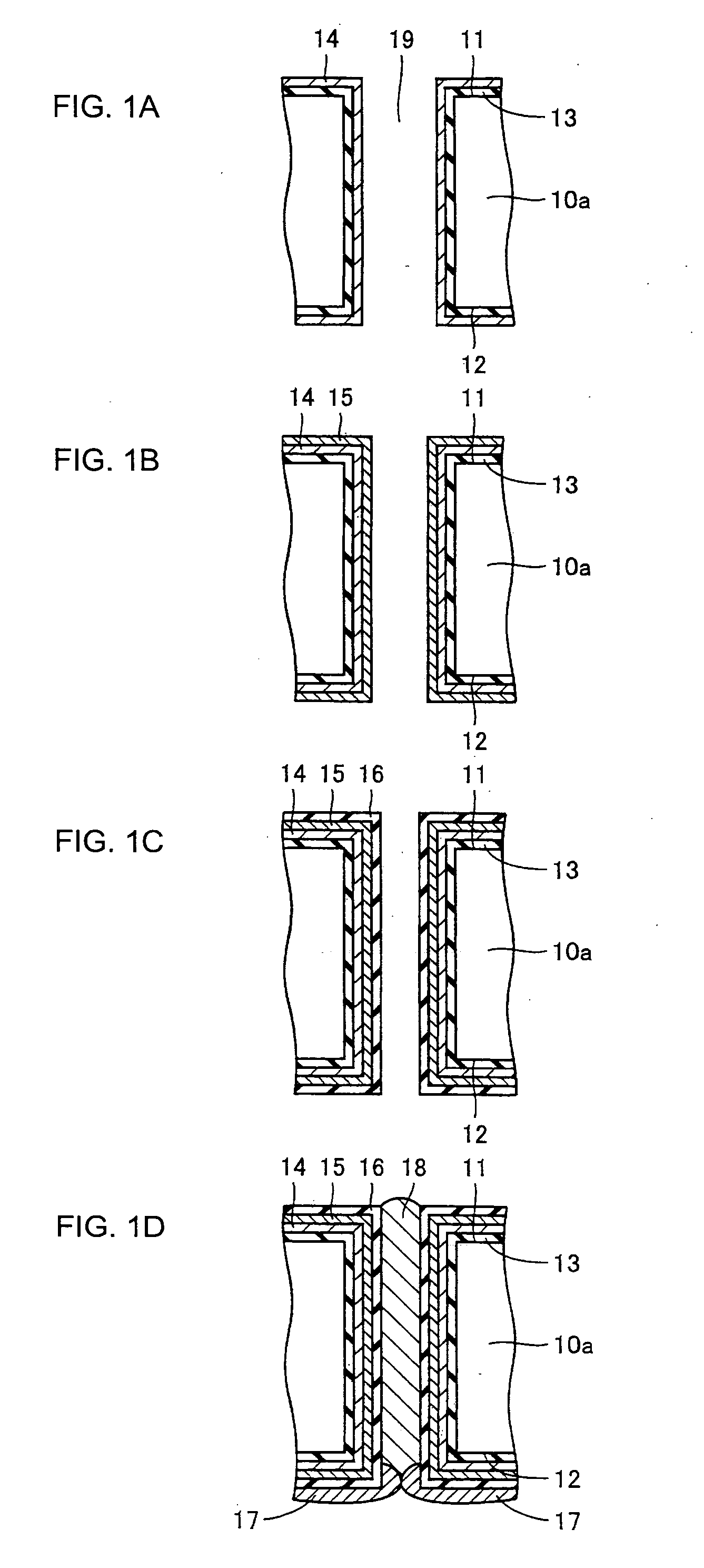
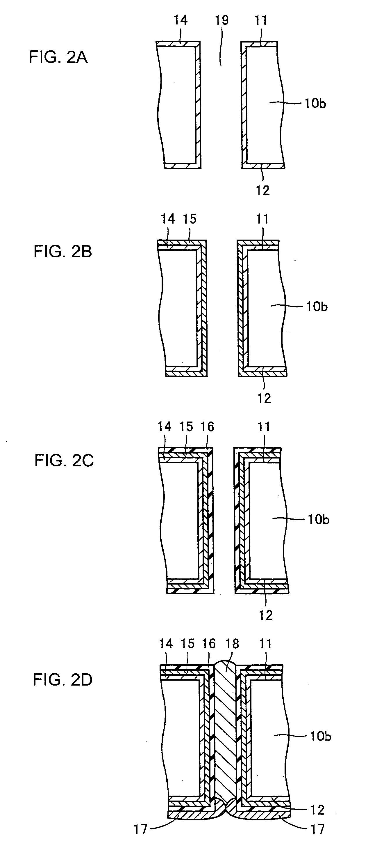
[0047] One embodiment of the present invention will be described with reference to the drawings hereinafter. FIGS. 1A to 1D show manufacturing steps of a through substrate according to one embodiment of the present invention step by step. Here, the through substrate means a substrate having a through hole provided from the front surface to the back surface of the substrate and includes a printed circuit board (including a flexible printed circuit board) and an interposer (including a silicon interposer).

[0048] Referring to FIG. 1, first, a silicon substrate (through substrate) 10 having a front surface 11 and a back surface 12 and comprises a plurality of through holes provided between both surfaces is prepared. In addition, the whole substrate 10 is covered with a silicon oxide film 13. Then, a Zn layer 14 is formed inside the through hole 19 and around the front and back surfaces by electroless plating (FIG. 1A). Then, a Cu layer 15 is formed on the Zn layer 14 by electroless pla...


PUM

PropertyMeasurementUnit
Electrical conductoraaaaaaaaaa
aaaaaaaaaa

Abstract

A through substrate which comprises a silicon substrate (10) having a through hole (19) penetrating a front surface (11) and a back surface (12), a oxidized silicon film (13) being provided along the inner wall surface of the through hole (19), layers (14, 15) comprising Zn and Cu, respectively, being formed on the inner wall surface of the oxidized silicon film (13), and a Cu plating layer (18) which has been grown from a Cu seed layer (17) along the inner wall surface of layers (14, 15) comprising Zn and Cu, respectively, via an insulating layer (16) between them. The above through substrate can provide a through electrode capable of avoiding the noise due to the cross talk.

Description

TECHNICAL FIELD [0001] The present invention relates to a through substrate, an interposer and a manufacturing method of the through substrate, and more particularly, to a through substrate and an interposer that can be used as a signal-flow path, and a manufacturing method of the through substrate. BACKGROUND ART [0002] A conventional multilayer wiring circuit substrate has a problem in that a crosstalk noise is generated in signal wirings because signal lines are close to each other due to high density of wiring layers, and an operation defect is generated in a driving element of the circuit. A method to solve the above problem is disclosed in Japanese Unexamined Patent Publication No. 2004-63725, for example. [0003] According to that document, a coaxial line having a coaxial structure is formed in a substrate and used as a signal wiring layer. [0004] The conventional method of eliminating the crosstalk noise has been performed as described above. However, there is a problem in th...

Claims


Application Information

Patent Timeline
IPC IPC(8): H05K1/11H05K3/10
CPCH01L21/486Y10T29/49165H01L23/147H01L23/481H01L23/49827H01L23/552H01L2223/6622H05K1/0222H05K1/0306H05K3/423H05K2201/09809H05K2203/0733H01L2924/0002H01L21/76898H01L2924/00H01L23/12
Inventor YAKABE, MASAMIKAGAWA, KENICHIHOSHINO, TOMOHISA
Owner TOKYO ELECTRON LTD
Why Eureka
Try Eureka