

Field programmable semiconductor object array integrated circuit
a technology of object arrays and integrated circuits, which is applied in the direction of logic circuits, semiconductor devices, pulse techniques, etc., can solve the problems of increasing the processing potential made possible by the increase in the density of transistors, increasing the cost and complexity of application specific integrated circuit (asic) development, and facilitating rapid design and implementation of higher-level functionality. , the effect of reducing the complexity of timing closur
- Summary
- Abstract
- Description
- Claims
- Application Information
AI Technical Summary
Benefits of technology
Problems solved by technology
Method used
Image

Examples
Embodiment Construction
Overview
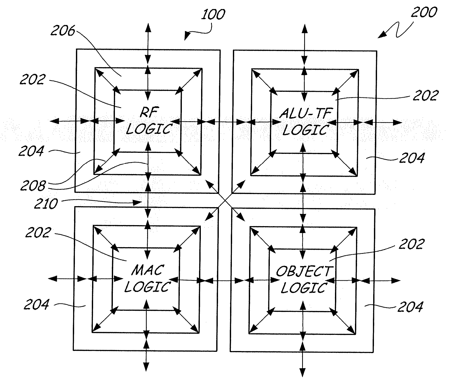
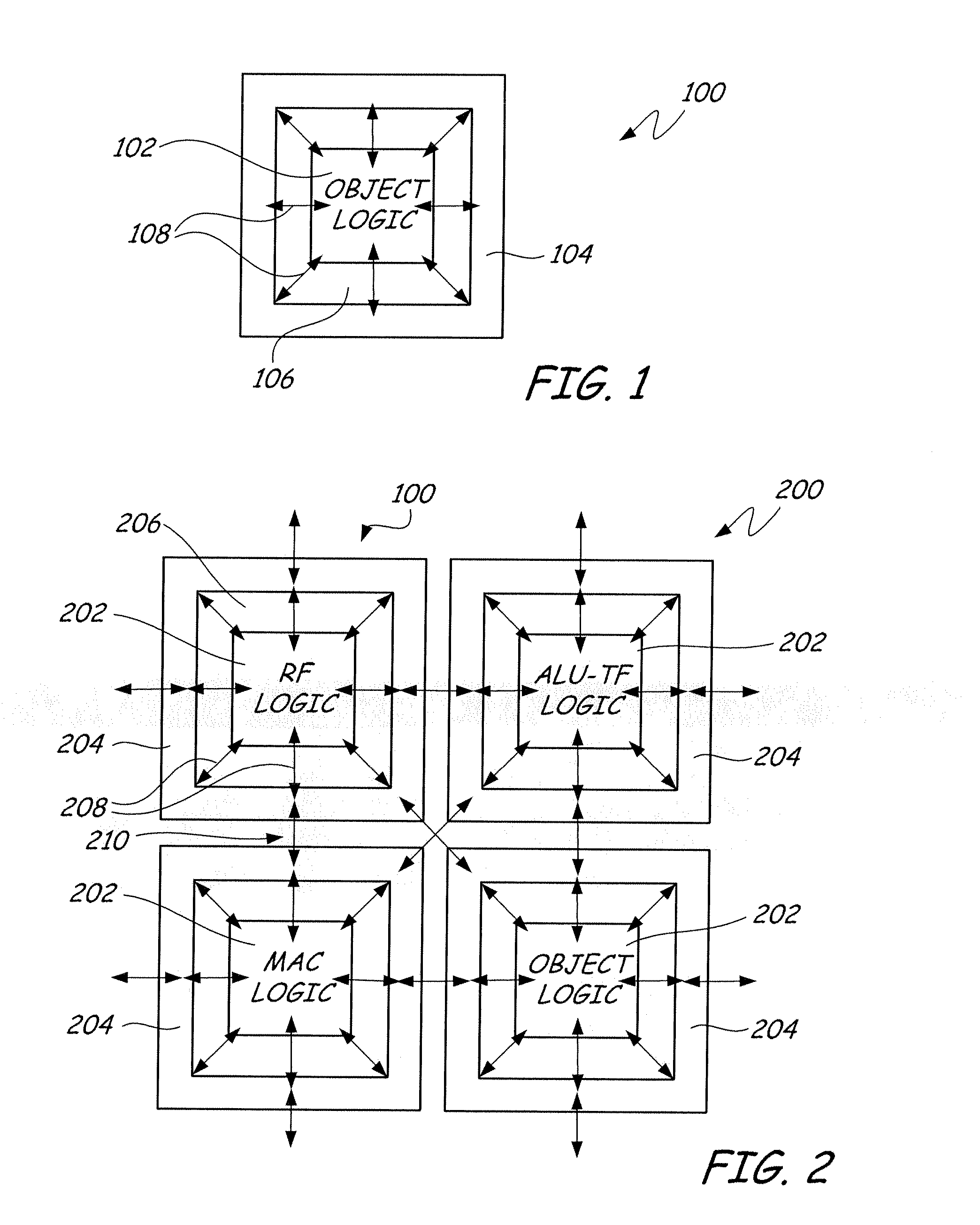
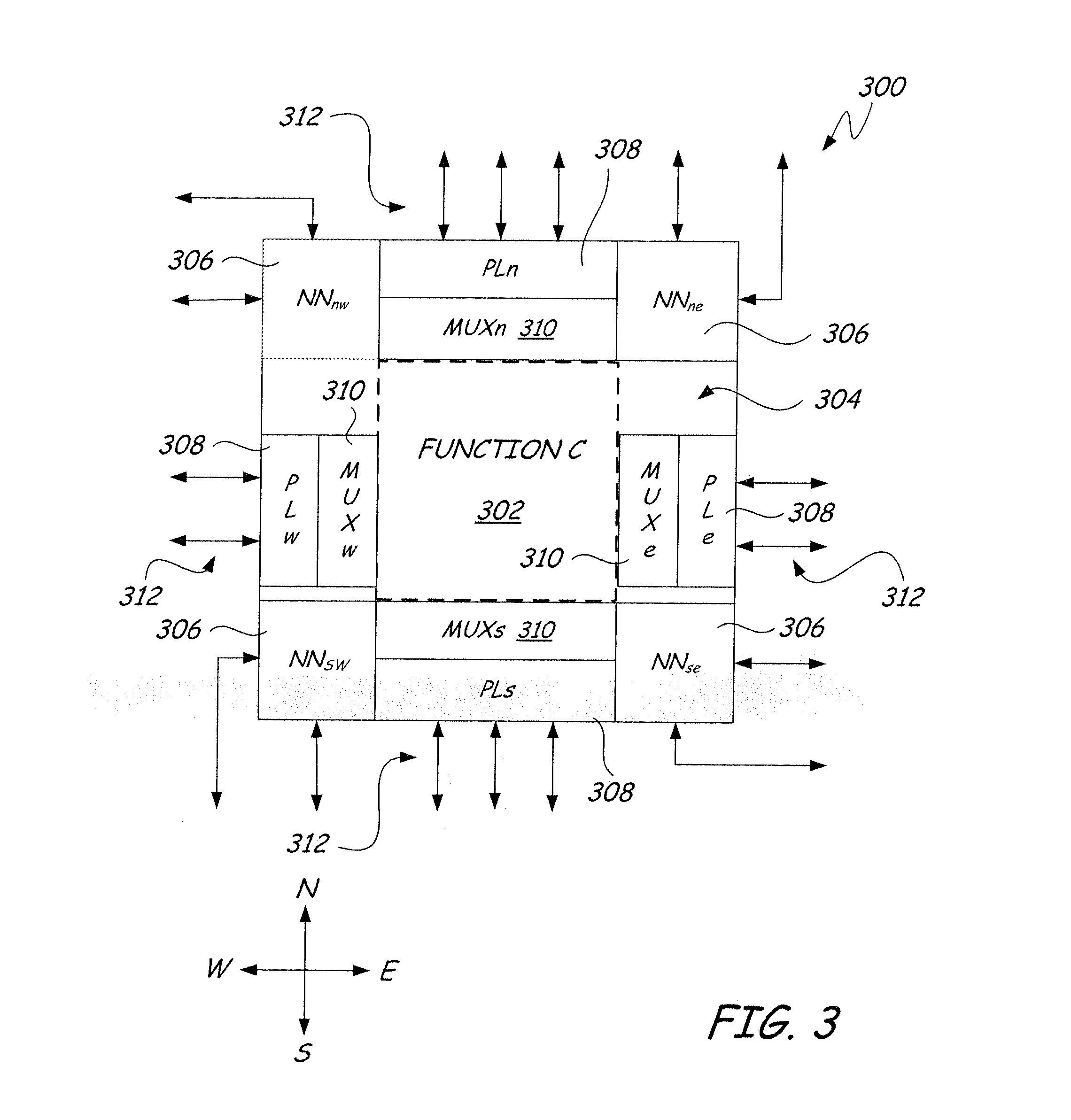
[0037] A field-programmable object array or FPOA is a medium grain architecture comprising highly optimized silicon objects that are individually programmed and synchronously interconnected via high performance parallel communications structures, permitting the user to configure the device to implement a variety of very high performance algorithms. The high level functions available in the objects combined with the unique interconnect structure enables performance superior to existing field programmable solutions while maintaining and enhancing the flexibility.
[0038] Aspects of the invention include but are not limited to the following: Optimized silicon object architecture with abutment design, synchronous array of silicon objects, combined Nearest Neighbor and Party Line inter-object communications, predictable place and route timing, object level power control, and object-level end user programmability.
[0039] In general, an FPOA can be described as a massively parallel...
PUM
 Abstract
Description
Claims
Application Information