Pixel circuit, display and driving method thereof

a technology of pixel circuit and driving method, which is applied in the direction of static indicating devices, heater elements, instruments, etc., can solve the problems of spoiled uniformity of screen, and difficult to fabricate large-size and high-definition displays, etc., to achieve high mobility, output current, and large mobility

Inactive Publication Date: 2007-10-25
SONY CORP
View PDF5 Cites 52 Cited by
  • Summary
  • Abstract
  • Description
  • Claims
  • Application Information

AI Technical Summary

Benefits of technology

[0015] According to another embodiment, correction of the input voltage held by the capacitive part is during a beginning portion of an emission period to cancel dependence of the output current on a carrier mobility of the drive transistor.
[0017] According to certain embodiments of the present invention, a pixel circuit includes a correction unit that corrects an input voltage (gate voltage) for a drive transistor to cancel the dependence of the output current from the drive transistor on the carrier mobility. This may, for example, be accommodated by negatively feeding back the output current to the capacitive part to correct the input voltage (gate voltage). As is apparent from Equation 1, the output current (drain current) is proportional to the mobility. Therefore, when a drive transistor in a certain pixel has a high mobility, the output current from the drive transistor is correspondingly large. This output current is negatively fed back to the capacitive part to thereby correct the input voltage (gate voltage). A larger mobility results in a larger negative feedback amount, and therefore the input voltage (gate voltage) is greatly decreased correspondingly. This decrease of the gate voltage results in suppression of the drain current. In contrast, when a drive transistor in another pixel is relatively small, the drain current from the drive transistor is also small. Therefore, the amount of negative feedback to a capacitive part is also small, which leads to a small decrease of the gate voltage. That is, a smaller mobility of a drive transistor provides a smaller output current, which results in a smaller amount of correction.

Problems solved by technology

The simple-matrix system employs a simple configuration, but involves difficulties of fabricating large-size and high-definition displays.
Thus, the luminance varies depending on each pixel, which spoils uniformity of the screen.
As a result, emission luminance varies from pixel to pixel, which problematically spoils uniformity of a screen.

Method used


Image

  • Pixel circuit, display and driving method thereof
  • Pixel circuit, display and driving method thereof
  • Pixel circuit, display and driving method thereof

Examples


Embodiment Construction

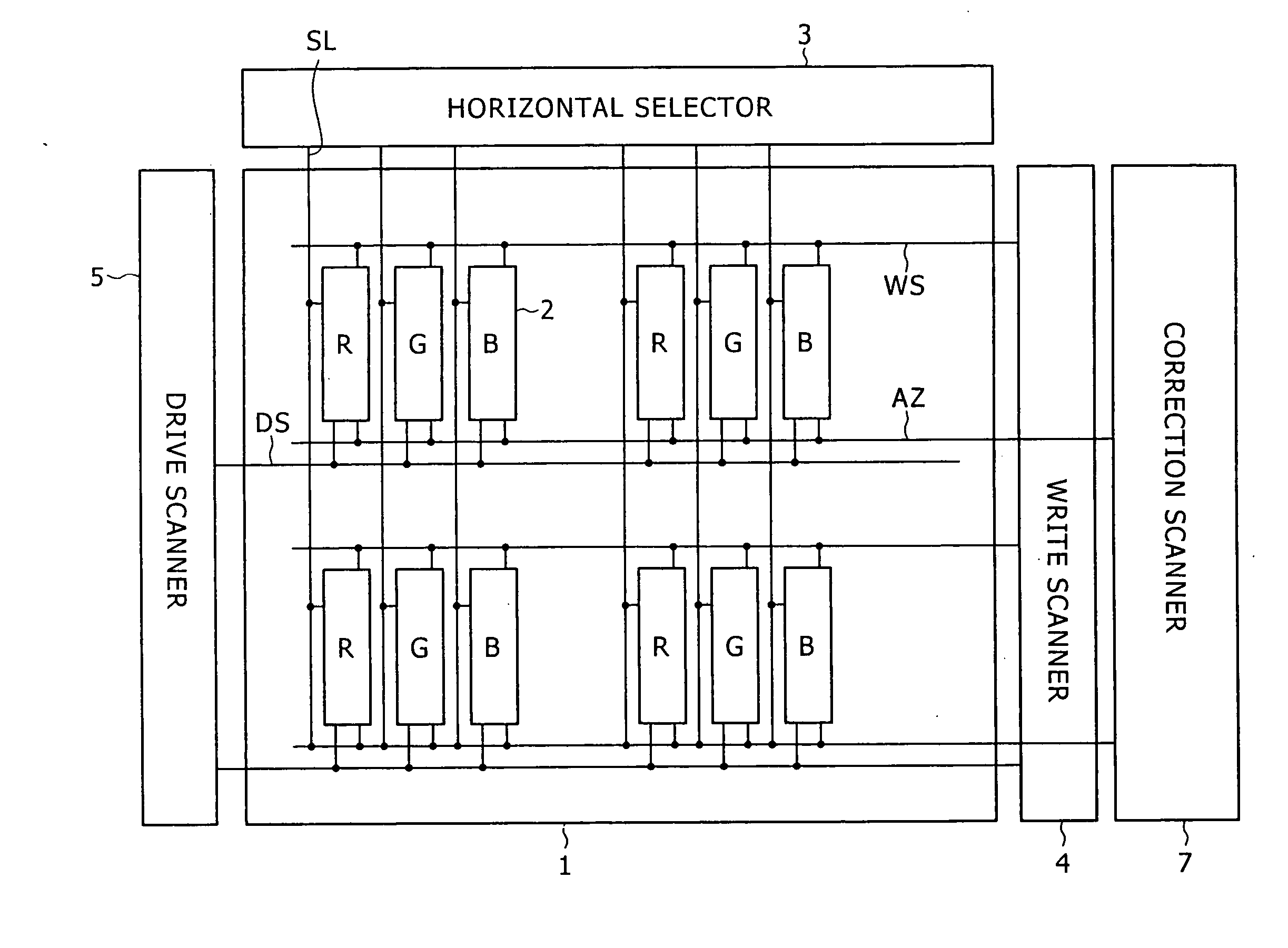
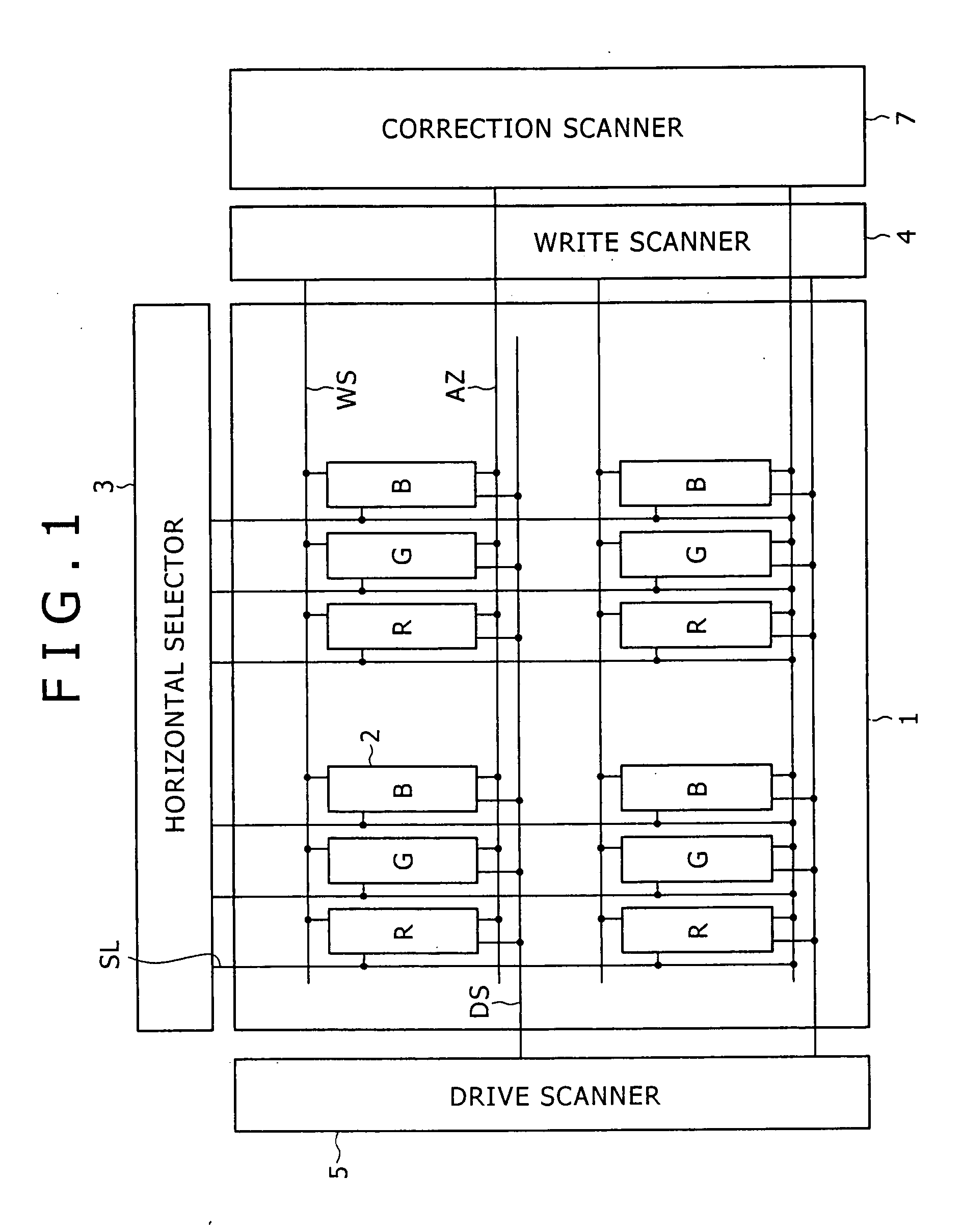
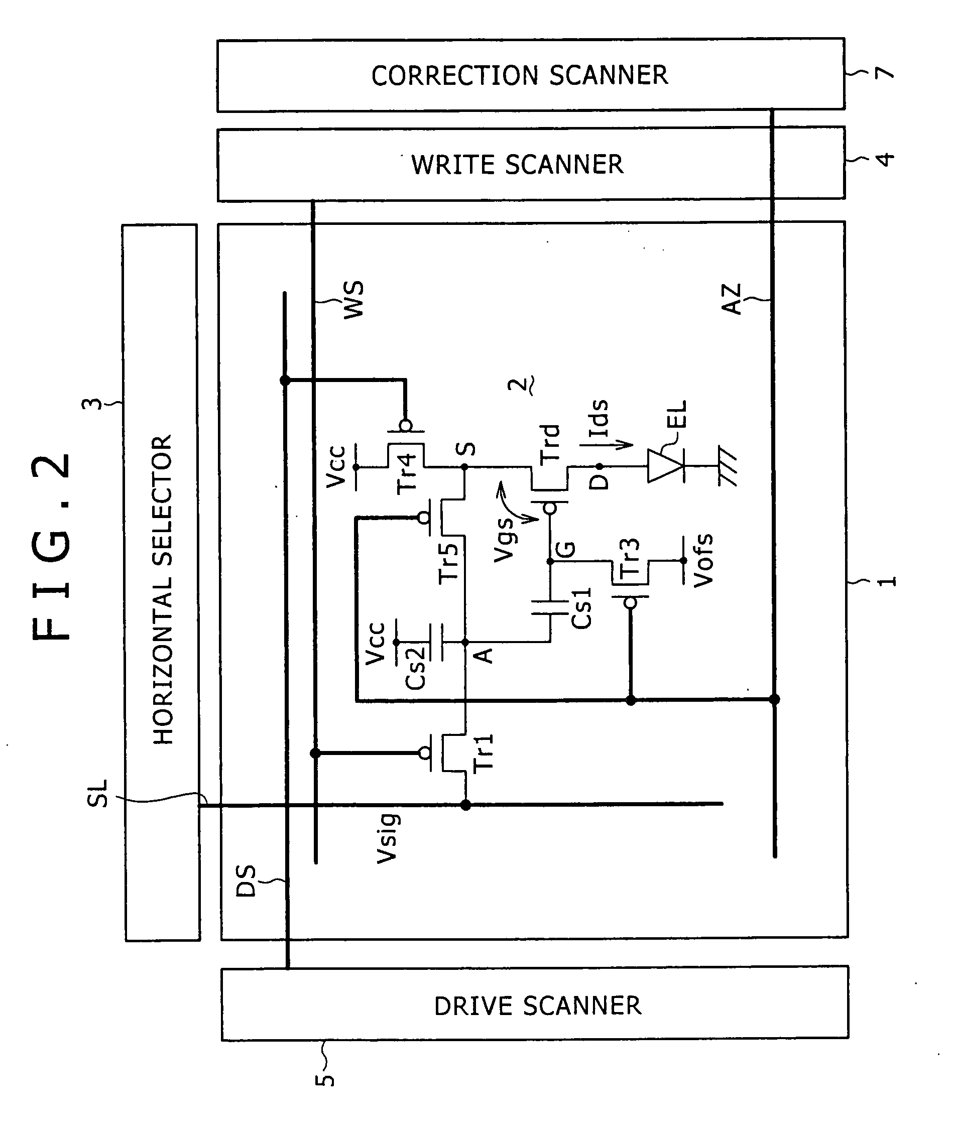
[0038] Embodiments of the present invention will be described below in detail with reference to the accompanying drawings. Initially, in order to clearly show the background of the invention, a reference example of an active-matrix display having a function of correcting the threshold voltage Vth will be described with reference to FIG. 1. Referring to FIG. 1, the active-matrix display includes a pixel array 1 that is a major part, and a peripheral circuit part. The peripheral circuit part includes a horizontal selector 3, a write scanner 4, a drive scanner 5, a correction scanner 7, and so on. The pixel array 1 includes pixels R, G and B that are disposed at the intersections between row scan lines WS and column signal lines SL, and thus are arranged in a matrix. Although pixels of three primary colors of RGB are used to allow color displaying in the example, the present invention is not limited thereto. Each of the pixels R, G and B is formed of a pixel circuit 2. The signal lines...


PUM


Abstract

The invention provides a pixel circuit that can cancel the influence of the mobility of a drive transistor. A drive transistor supplies a light-emitting element with an output current dependent upon an input voltage. The light-emitting element emits light with a luminance dependent upon a video signal in response to the output current supplied from the drive transistor. The pixel circuit includes a correction unit that corrects the input voltage held by a capacitive part in order to cancel the dependence of the output current on the carrier mobility.

Description

CROSS REFERENCE TO RELATED APPLICATIONS [0001] This application is a continuation of U.S. application Ser. No. 11 / 338,631 filed on Jan. 25, 2006, and also claims priority to Japanese Patent Application JP 2005-027028 filed in the Japanese Patent Office on Feb. 2, 2005. The entire contents of these applications are hereby incorporated by reference.BACKGROUND OF THE INVENTION [0002] The present invention relates to a pixel circuit for current-driving a light-emitting element provided for each pixel. The invention also relates to a display that includes the pixel circuits arranged in a matrix (in rows and columns), and particularly to an active-matrix display that employs insulated-gate field effect transistors provided in the respective pixel circuits and controlling the amount of a current applied to a light-emitting element, such as an organic electro-luminescence (EL) element. [0003] In an image display, e.g., in a liquid crystal display, a number of liquid crystal pixels are arran...

Claims


Application Information

Patent Timeline
Patent Type & Authority Applications(United States)
IPC IPC(8): G09G3/14H05B44/00
CPCG09G3/3233G09G2300/0819G09G2300/0842G09G2320/045G09G2300/0861G09G2310/061G09G2320/043G09G2300/0852H05B3/347H05B3/08G09G3/3266G09G5/10G09G5/18
Inventor YAMASHITA, JUNICHIUCHINO, KATSUHIDE
Owner SONY CORP
Why Eureka
Try Eureka