

Vertical and trench type insulated gate mos semiconductor device
a technology of insulating gate and semiconductor device, which is applied in the direction of semiconductor/solid-state device manufacturing, semiconductor devices, electrical apparatus, etc., can solve the problems of low turn-off capability, difficult to lower the on-voltage with a high current density, and inability to form the current path of the trench sidewall in the lateral direction. , to achieve the effect of enhancing the turn-off capability and lowering the resistan
- Summary
- Abstract
- Description
- Claims
- Application Information
AI Technical Summary
Benefits of technology
Problems solved by technology
Method used
Image

Examples
example 1
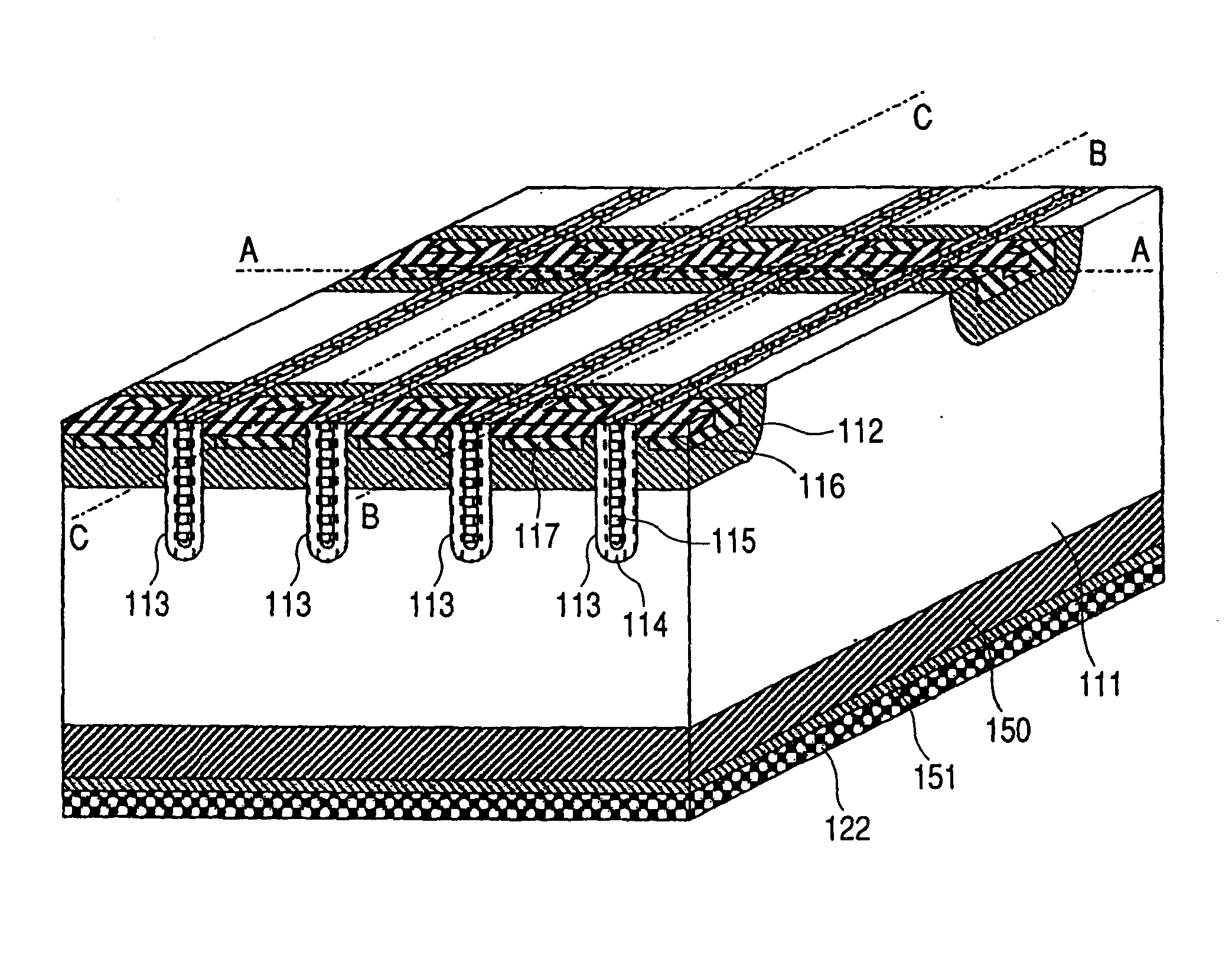
[0149] In the following, Example 1 of the vertical and trench type insulated gate MOS semiconductor device according to the invention will be explained with reference to FIG. 1 to FIG. 9, FIG. 13 and FIG. 14. In Example 1, a vertical IGBT with a breakdown voltage of 600V is taken as an example of a power vertical and trench type insulated gate MOS semiconductor device and its manufacturing process will be explained.
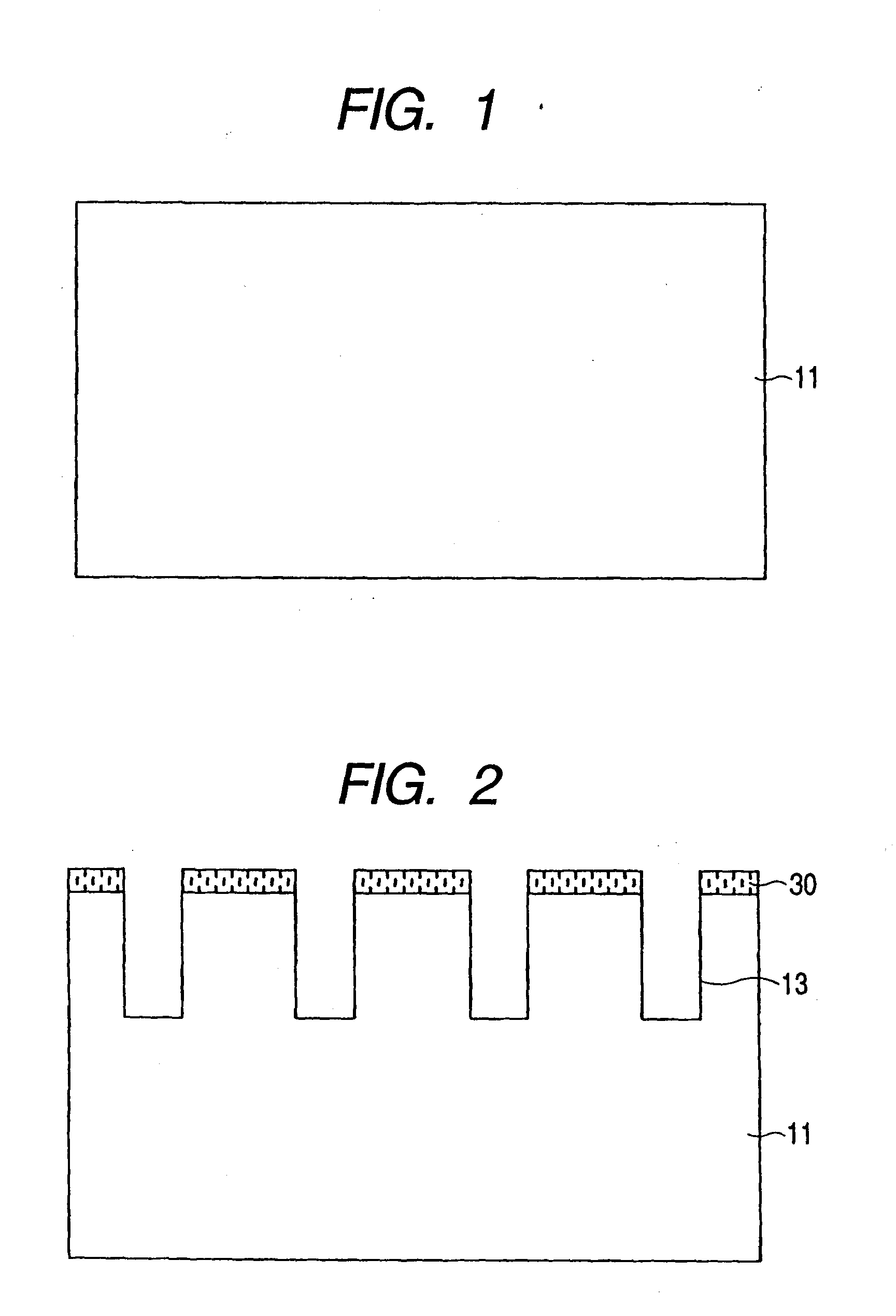
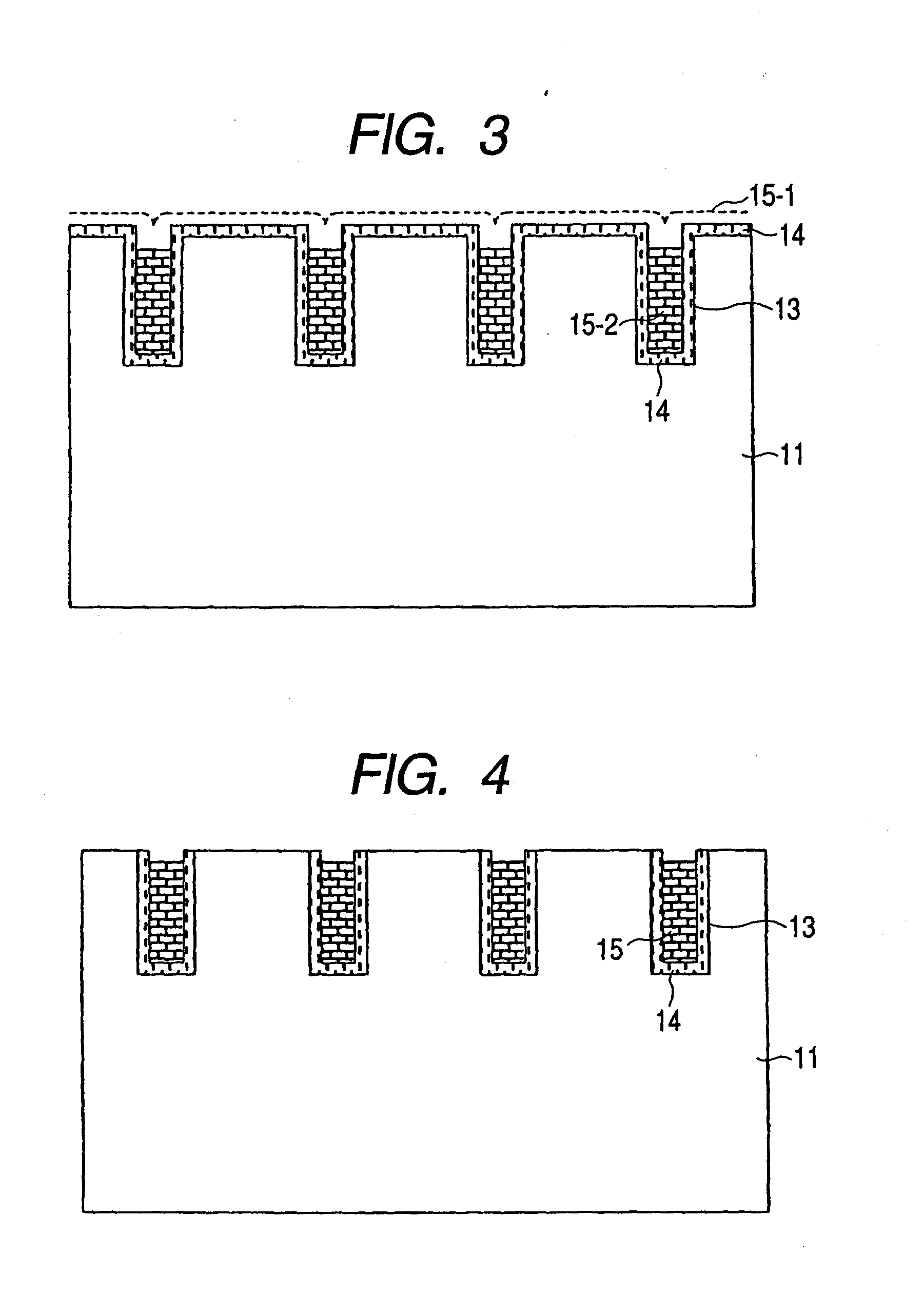
[0150] As in a related device, n−-type silicon substrate 11 is prepared as shown in FIG. 1. N−-type silicon substrate 11 has an n−-region that becomes a base region on the surface thereof whose direction of crystal plane is (100) and has a resistivity of 30 Ωcm. On the surface of n−-type silicon substrate 11, a resist pattern is formed for forming a guard ring (a kind of a voltage blocking structure with a function of reducing electric field strength on a surface—not shown), p-type impurity ions are implanted, and heat treatment is carried out after the resist is removed...
example 2
[0162] Example 2 of the vertical and trench type insulated gate MOS semiconductor device according to the invention will be explained with reference to FIG. 15. In Example 2, a vertical IGBT with a breakdown voltage of 600 V is taken as an example of a power vertical and trench type insulated gate MOS semiconductor device and its structure will be shown.
[0163] The process of manufacturing the IGBT is the same as that in Example 1 with only the shapes, arrangements and dimensions of p+-type body region 27, n+-type emitter region 26 and contact region 41 of a metal / semiconductor layer being modified from those in Example 1. The main modification is that the angle formed by trench 13 and a side of n+-type emitter region 26 intersecting trench 13 is 45 degrees rather than 90 degrees and that the length of contact region 41 of the metal / semiconductor layer in the longitudinal direction of trench 13 is longer than the length of n+-type emitter region 26 in the longitudinal direction of t...
example 3
[0166] Example 3 of the vertical and trench type insulated gate MOS semiconductor device according to the invention will be explained with reference to FIG. 16. In Example 3, a vertical IGBT with a breakdown voltage of 600 V is taken as an example of a power vertical and trench type insulated gate MOS semiconductor device and its structure will be shown.
[0167] The process of manufacturing the IGBT is the same as that in Example 1 with only the shapes, arrangements and dimensions of p+-type body region 37, n+-type emitter region 36 and contact region 42 of a metal / semiconductor layer being modified from those in Example 1. The main modification is that the angle formed by trench 13 and a side of n+-type emitter region 36 intersecting trench 13 is 45 degrees rather than 90 degrees and that contact region 42 of the metal / semiconductor layer is not provided for all of the portions in the longitudinal direction of trench 13 of n+-type emitter region 36. With contact region 42 of the met...
PUM
 Abstract
Description
Claims
Application Information