

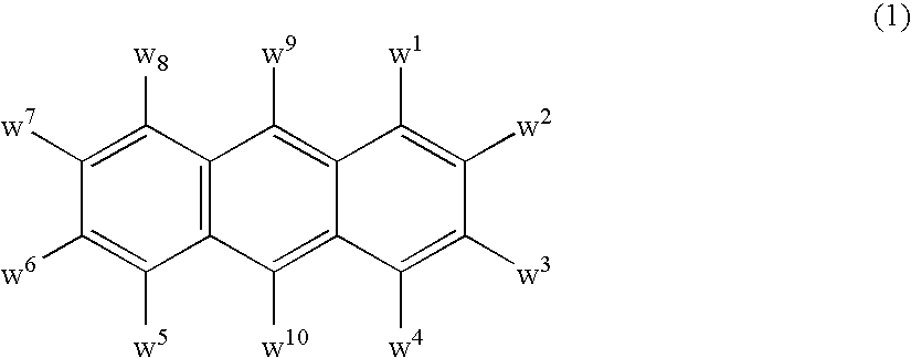
Electroluminescent device including an anthracene derivative
a technology of electroluminescent devices and derivatives, applied in the direction of luminescent screens, organic semiconductor devices, discharge tubes, etc., can solve the problems of device performance limitations, many desirable applications, and may not yield the most desirable electroluminescent properties, etc., to achieve the effect of improving electroluminescent properties, driving voltage and efficiency
- Summary
- Abstract
- Description
- Claims
- Application Information
AI Technical Summary
Benefits of technology
Problems solved by technology
Method used
Image

Examples
example 1
Electrochemical Redox Potentials and Estimated Energy Levels
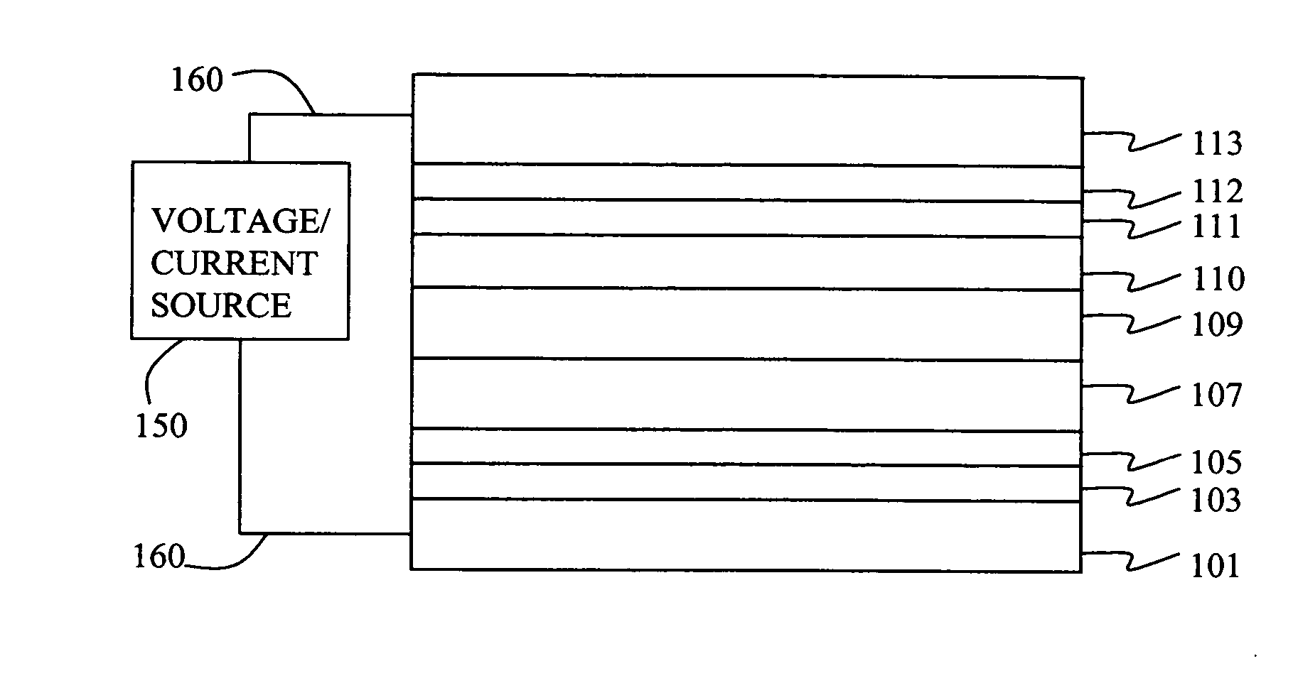
[0174] LUMO and HOMO values are typically estimated experimentally by electrochemical methods. The following method illustrates a useful means to measure redox properties. A Model CHI660 electrochemical analyzer (CH Instruments, Inc., Austin, Tex.) was employed to carry out the electrochemical measurements. Cyclic voltammetry (CV) and Osteryoung square-wave voltammetry (SWV) were used to characterize the redox properties of the compounds of interest. A glassy carbon (GC) disk electrode (A=0.071 cm2) was used as working electrode. The GC electrode was polished with 0.05 μm alumina slurry, followed by sonication cleaning in Milli-Q deionized water twice and rinsed with acetone in between water cleaning. The electrode was finally cleaned and activated by electrochemical treatment prior to use. A platinum wire served as counter electrode and a saturated calomel electrode (SCE) was used as a quasi-reference electrode to complet...
example 2
Fabrication of Device 1-1 through 1-11
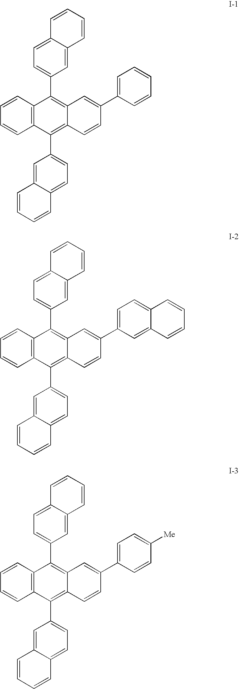
[0178] A series of EL devices (1-1 through 1-11) were constructed as described below. [0179] 1. A glass substrate coated with a 25 nm layer of indium-tin oxide (ITO), as the anode, was sequentially ultrasonicated in a commercial detergent, rinsed in deionized water, degreased in toluene vapor and exposed to oxygen plasma for about 1 min. [0180] 2. Over the ITO was deposited a 1 nm fluorocarbon (CFx) hole-injecting layer (HIL) by plasma-assisted deposition of CHF3 as described in U.S. Pat. No. 6,208,075. [0181] 3. Next a layer of hole-transporting material 4,4′-Bis[N-(1-naphthyl)-N-phenylamino]biphenyl (NPB) was deposited to a thickness of 75 nm. [0182] 4. A light-emitting layer (LEL) corresponding to a host material I-1 and including light-emitting material, D-1, at level of 0.75% of the layer by volume was deposited to a thickness of 20.0 nm over the HTL. [0183] 5. An electron-transporting layer (ETL) composed of rubrene or I-1 (see Table 2a) ...
example 3
Fabrication of Device 2-1 through 2-12
[0189] A series of EL devices (2-1 through 2-12) were constructed in the same manner as device 1-1, as described below. [0190] 1. A glass substrate coated with a 25 nm layer of indium-tin oxide (ITO), as the anode, was sequentially ultrasonicated in a commercial detergent, rinsed in deionized water, degreased in toluene vapor and exposed to oxygen plasma for about 1 min. [0191] 2. Over the ITO was deposited a 1 nm fluorocarbon (CFx) hole-injecting layer (HIL) by plasma-assisted deposition of CHF3 as described in U.S. Pat. No. 5 6,208,075. [0192] 3. Next a layer of hole-transporting material 4,4′-Bis[N-(1-naphthyl)-N-phenylamino]biphenyl (NPB) was deposited to a thickness of 75 nm. [0193] 4. A light-emitting layer (LEL) corresponding to a host material I-1, TBADN or Alq and including light-emitting material D-1 or D-2 was deposited to a thickness of either 20 nm or 40 nm over the HTL. See Table 3a for a description of the LEL host, dopant, and t...
PUM
| Property | Measurement | Unit |
|---|---|---|
| thickness | aaaaa | aaaaa |
| LUMO energy | aaaaa | aaaaa |
| thick | aaaaa | aaaaa |
Abstract
Description
Claims
Application Information