Nano-enhanced raman spectroscopy substrate packaging structure

a raman spectroscopy and substrate technology, applied in the direction of spectrometry/spectrophotometry/monochromators, optical radiation measurement, instruments, etc., can solve the problems of ners substrate being easily contaminated, unable to maintain the pristine state of the substrate before it is deployed, and expensive laser sources used

Active Publication Date: 2007-11-01
HEWLETT PACKARD DEV CO LP
View PDF10 Cites 55 Cited by
  • Summary
  • Abstract
  • Description
  • Claims
  • Application Information

AI Technical Summary

Benefits of technology

[0014] While the specification concludes with claims particularly pointing out and distinctly claiming that which is regarded as the present invention, the advantages of this invention can be more readily ascertained from the following description of the invention when read in conjunction with the accompanying drawings in which:

Problems solved by technology

As a result, powerful, costly laser sources typically are used to generate high intensity excitation radiation to increase the otherwise weak Raman signal for detection.
The NERS substrate may be easily contaminated.
Maintaining the pristine state of the substrate before it is deployed may be difficult.
One solution is a disposable NERS substrate; however, this may be expensive.

Method used


Image

  • Nano-enhanced raman spectroscopy substrate packaging structure
  • Nano-enhanced raman spectroscopy substrate packaging structure
  • Nano-enhanced raman spectroscopy substrate packaging structure

Examples


first embodiment

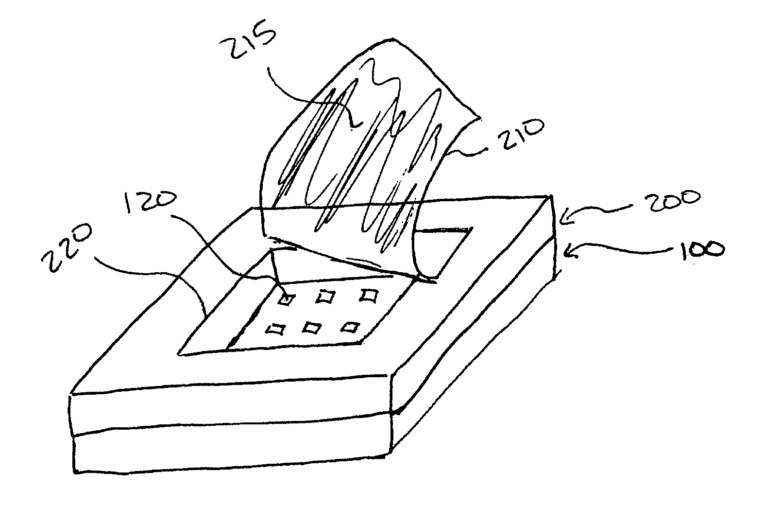
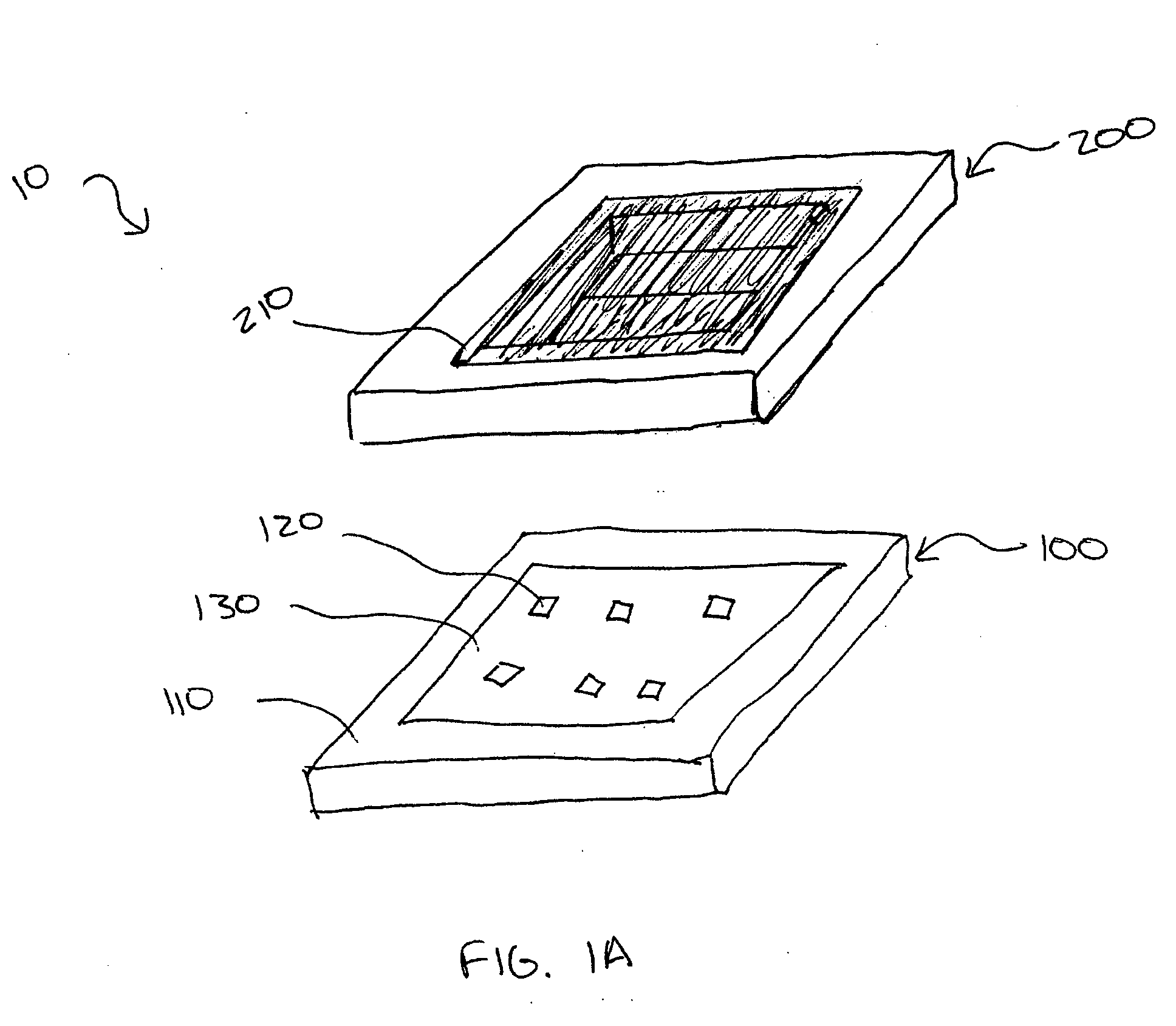
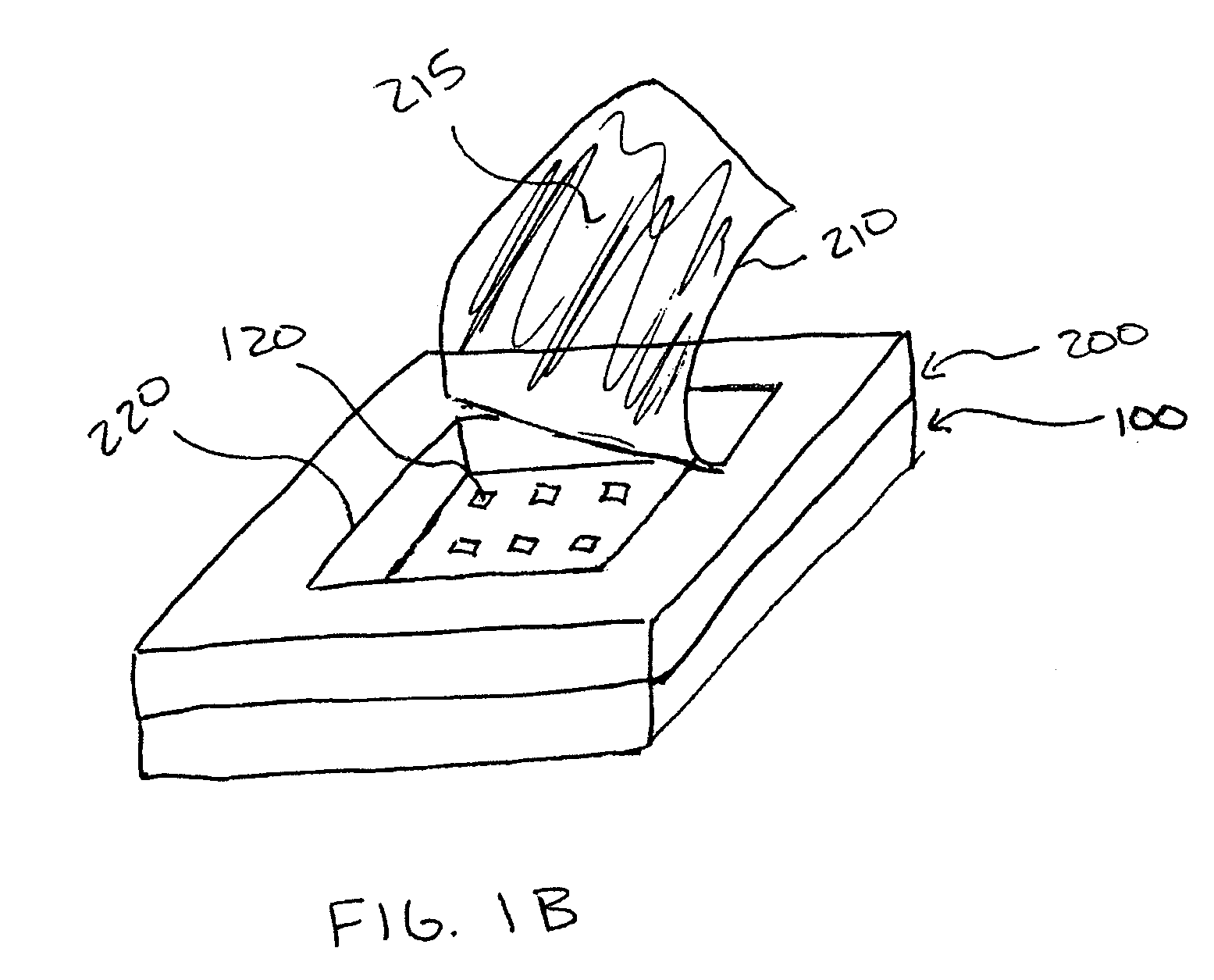
[0024] a packaged NERS-active structure 10 according to the invention is shown in FIGS. 1A and 1B. FIG. 1A depicts the packaged NERS-active structure 10 in an exploded view, and FIG. 1B illustrates the packaged NERS-active structure 10 in assembled form. The packaged NERS-active structure 10 includes a NERS-active substrate 100 and a packaging substrate 200. The NERS-active substrate may comprise, by way of example, one of silicon, glass, quartz or plastic material. The NERS-active substrate 100 may include at least one NERS-active structure 120 on a first surface 110 thereof. FIG. 1A depicts a plurality of NERS-active structures 120 disposed on the first surface 110 in an array. Optionally, the plurality of NERS-active structures 120 may be randomly positioned. The at least one NERS-active structure 120 may be on a central region 130 of the substrate first surface 110. The NERS-active structures 120 may be formed of a NERS-active material, such as, for example gold, silver, copper,...

second embodiment

[0030]FIG. 2 depicts a packaged NERS substrate of the present invention. A NERS coupon 300 may be formed of a substrate made of, for example, silicon, glass, quartz, or plastic, with an array of NERS sites 330 thereon. The NERS coupon 300 may be between about 1 cm2 to about 10 cm2 Each NERS site 330 may be between about 1 μm2 to about 200 μm2. Anywhere from one to several millions of NERS sites 330 may be disposed on the NERS coupon 300. Each NERS site 330 comprises at least one NERS-active structure 120, as shown in FIG. 1A.

[0031] A packaging substrate 400 may include a plurality of openings 420 therein. Each opening 420 may be covered with a membrane 410. The packaging substrate may include a first surface 430 and an opposing, second surface 440. The second surface may be adjacent to the NERS coupon 300. The membranes 410 may be disposed on the first surface 430. Each opening 420 may optionally be tapered, with the area of the opening 424 at the first surface 430 being less than t...


PUM

PropertyMeasurementUnit
poweraaaaaaaaaa
areaaaaaaaaaaa
areaaaaaaaaaaa

Abstract

Packaged NERS-active structures are disclosed that include a NERS substrate having a NERS-active structure thereon, and a packaging substrate over the NERS substrate having an opening therethrough, the opening in alignment with the NERS-active structure. A membrane may cover the opening in the packaging substrate. In order to perform nanoenhanced Raman spectroscopy, the membrane may be removed, and an analyte placed on the NERS substrate adjacent the NERS-active structure. The membrane may be replaced with another membrane after the analyte has been placed on the substrate. The membrane may maintain the pristine state of the substrate before it is deployed, and the replacement membrane may preserve the substrate and analyte for archival purposes. Also disclosed are methods for performing NERS with packaged NERS-active structures.

Description

FIELD OF THE INVENTION [0001] The invention relates to nanoenhanced Raman scattering (NERS). More particularly, the invention relates to packaging for NERS-active structures, protection for surfaces of NERS-active structures, also including methods for forming packaging for NERS-active structures, and methods for packaging NERS-active structures. BACKGROUND OF THE INVENTION [0002] Raman spectroscopy is a well-known technique for performing chemical analysis. In conventional Raman spectroscopy, high intensity monochromatic light provided by a light source, such as a laser, is directed onto an analyte (or sample) that is to be chemically analyzed. A majority of the incident photons are elastically scattered by the analyte molecule. In other words, the scattered photons have the same energy, and thus the same frequency, as the photons that were incident on the analyte. However, a small fraction of the photons (i.e., about 1 in 107 photons) are inelastically scattered by the analyte mol...

Claims


Application Information

Patent Timeline
Patent Type & Authority Applications(United States)
IPC IPC(8): G01N21/62
CPCG01N21/658Y10T428/218Y10T428/28
Inventor LI, ZHIYONGTONG, WILLIAM M.WILLIAMS, R. STANLEY
Owner HEWLETT PACKARD DEV CO LP
Why Eureka
Try Eureka