

Solar cell having doped semiconductor heterojunction contacts
a semiconductor heterojunction and contact technology, applied in the field of photovoltaic solar cells, can solve the problems of limited commercialization of ibc solar cells, limited efficiency of silicon photovoltaic cells in directly converting solar energy to electricity, and low cost effectiveness of process for conventional low-cost flat-plate solar panels
- Summary
- Abstract
- Description
- Claims
- Application Information
AI Technical Summary
Benefits of technology
Problems solved by technology
Method used
Image

Examples
Embodiment Construction
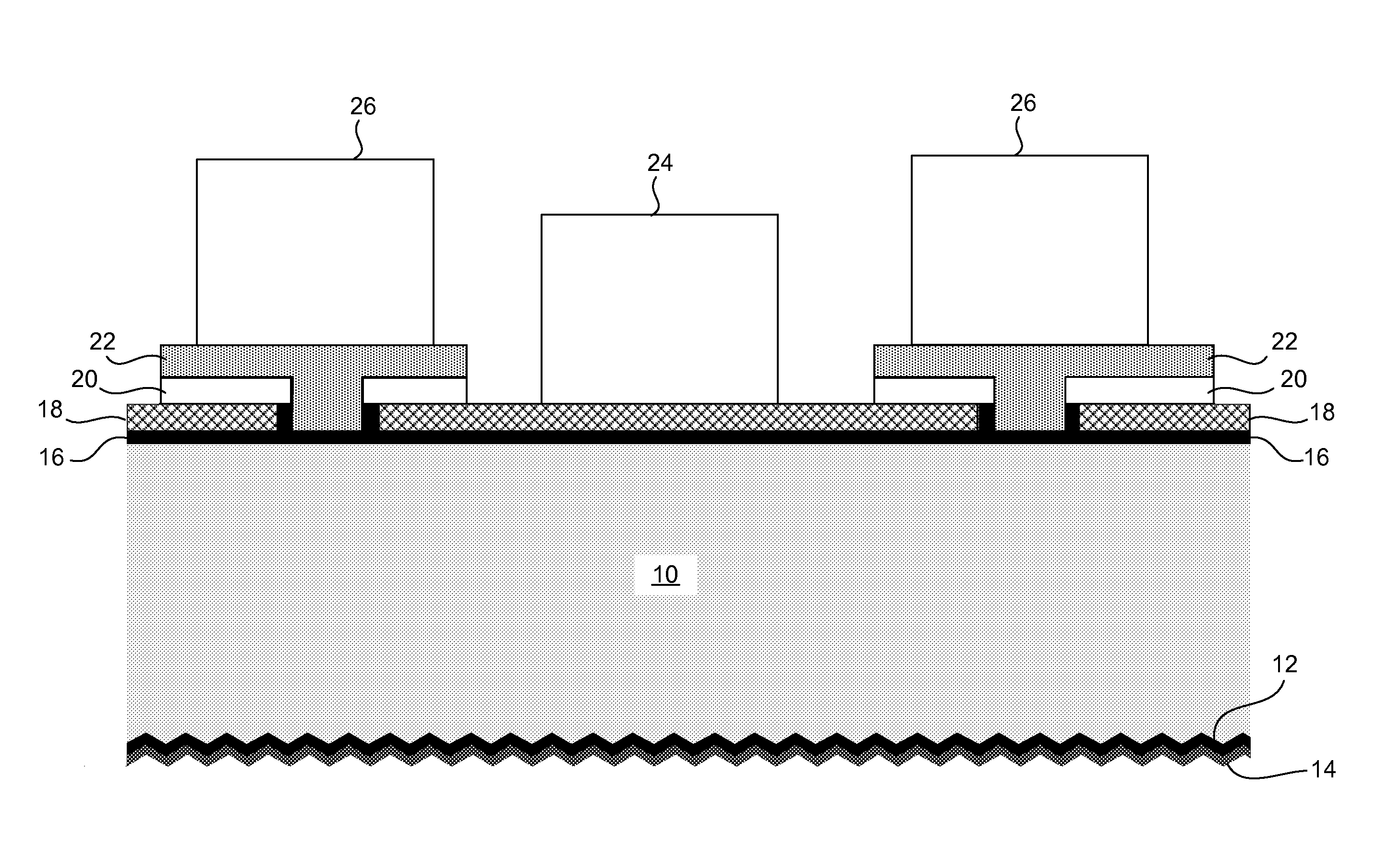
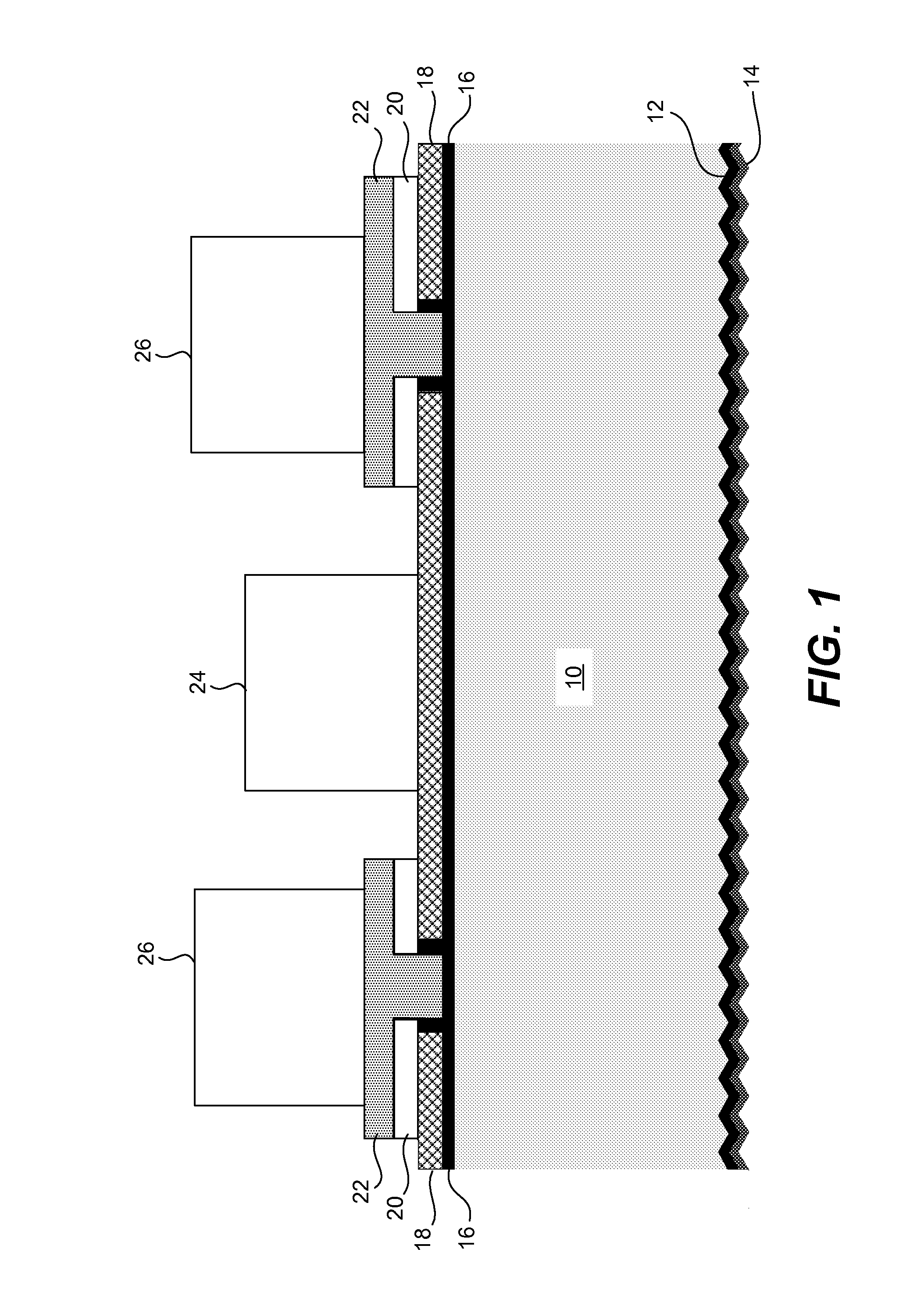
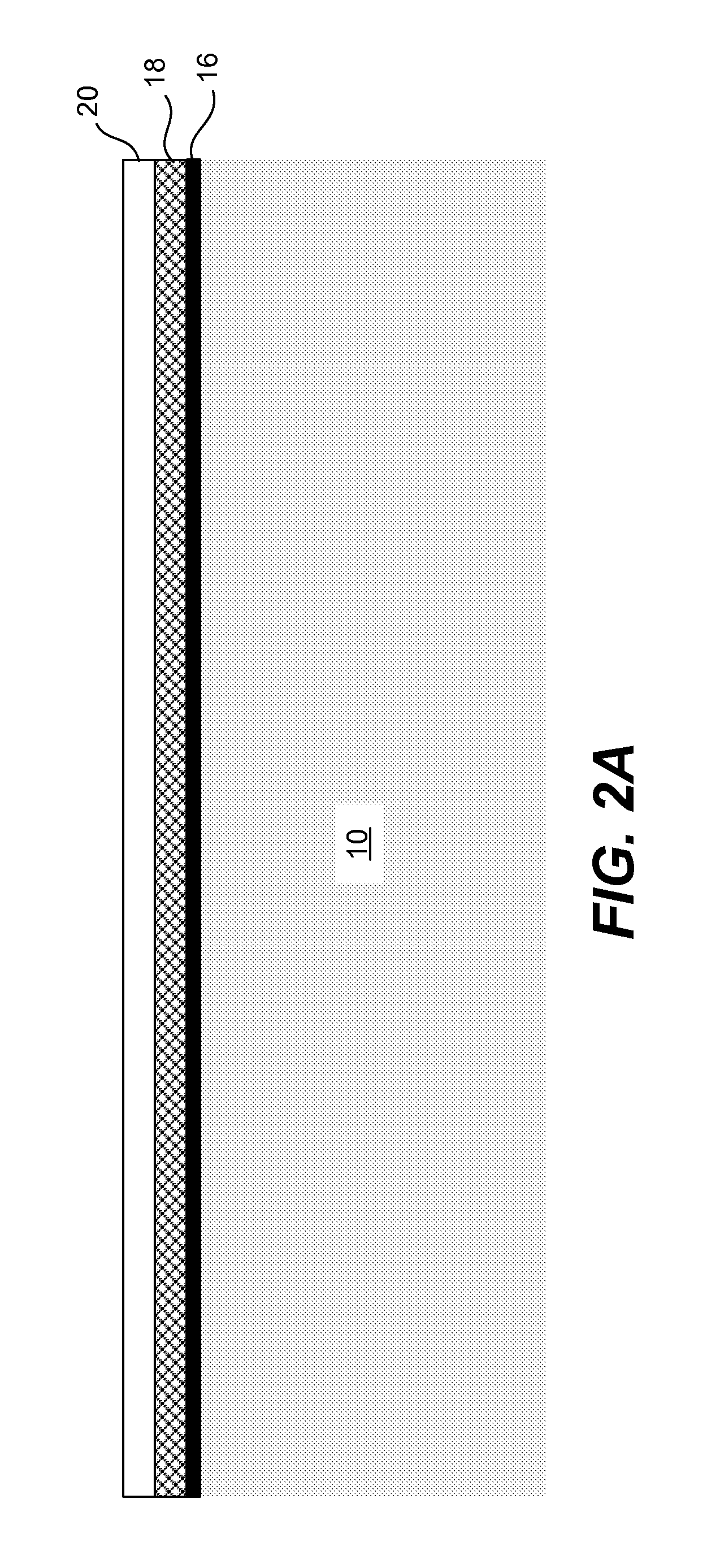
[0013] In accordance with one embodiment of the invention, an interdigitated back contact (IBC) solar cell comprising a silicon semiconductor body having first and second opposing major surfaces receives radiation through the first surface and has first and second patterns of acceptor doped amorphous silicon and donor doped amorphous silicon, respectively, on the second or back surface for receiving electron and hole carriers created in the silicon substrate by radiated photons. The structure is similar to prior art back contact solar cells which utilize doped P and N conductivity contacts formed in the substrates for receiving the holes and electrons created by radiation. However, the use doped P and N contacts in the substrate requires photoresist masking, etching, dopant diffusion, and high temperature processing in the fabrication of the solar cell. The use of acceptor and donor amorphous silicon contacts on the structure, in accordance with an embodiment of the invention, obvia...
PUM
 Abstract
Description
Claims
Application Information