Touch Screen Element

a touch screen element and touch screen technology, applied in the direction of electronic switching, pulse technique, instruments, etc., can solve the problems of reducing transparency, adding considerable expense, and affecting the effect of sensitivity

Inactive Publication Date: 2007-11-08
ATMEL CORP
View PDF22 Cites 395 Cited by
  • Summary
  • Abstract
  • Description
  • Claims
  • Application Information

AI Technical Summary

Benefits of technology

[0033]Another object of the invention is to provide for a driver circuit having low average power, for example by the use of sleep modes where the device samples slowly or not at all and mostly sleeps, and a wake function whereby when touched the device speeds up to provide appropriate speed of response.
[0034]Another object of the invention is to provide for proximity detection, so that the sensing surface can be made to react to non-touch, for example to provide a wakeup function for the product it is interfaced to, to bring it out of a low-power sleep state.

Problems solved by technology

Many types of 2DCT are known to suffer from a geometric distortion known as ‘pin-cushion’ whereby the reported coordinate of touch is in error due to electrical effects on the sensing surface.
U.S. Pat. No. 4,550,221 (Mabusth) is an example of a matrix approach where x and y oriented electrodes must cross each other, forcing the electrode structure to occupy two or more layers which adds considerable expense and in the case of LCD touch screens reduces transparency.
Co-pending U.S. Provisional Application 60 / 697,613 (published as GB2428306) further describes a method for structuring electrodes which avoid crossovers in the sensing region with little or no distortion, but this method still requires a relatively large number of connections.
These methods can all provide good resolution but require a large number of connections and are therefore costly to implement.
Also, a high connection count limits utility in smaller touch screens were there is little space surrounding the sensing area to permit large numbers of wiring traces to the connections.
2DCT devices which employ matrix or electrode-to-electrode coupling approaches such as U.S. Pat. No. 4,198,539 (Pepper) or U.S. Pat. No. 5,650,597 (Redmayne) also have a limited ability to project fields through thick materials, or to project their fields slightly into free space to create a ‘point screen’.
In the case of U.S. Pat. No. 4,198,539 (Pepper) the individual electrodes are very narrow and as a result have limited surface area which is essential to project a field through a thicker dielectric; as a result, such designs are typically limited in application to track pads for notebook computers and the like, with a thin overlay on top of electrodes.
Such limitations reduce touch signal strength and prevent the use of the electrodes with thick dielectric layers.
Such a calibration process adds to the cost of the sensing element and can easily fall out of calibration with time and environmental conditions, such as temperature or humidity or exposure to light, which over time can alter the resistance of the electrodes.
The need for recalibration of the sensing element is a serious commercial disadvantage.
The device cannot therefore detect a human touch.
One disadvantage of the y axis field gradient produced by this design is that the gain along the vertical axis is insufficient to provide full scale readings, thus requiring the output to be rescaled accordingly.
Also it is quite difficult to prevent the response from being granular as the patterns can be quite large to accomplish the desired gradient effect on the y axis.
This system is also incapable of detecting human touch.

Method used


Image

  • Touch Screen Element
  • Touch Screen Element
  • Touch Screen Element

Examples


first embodiment

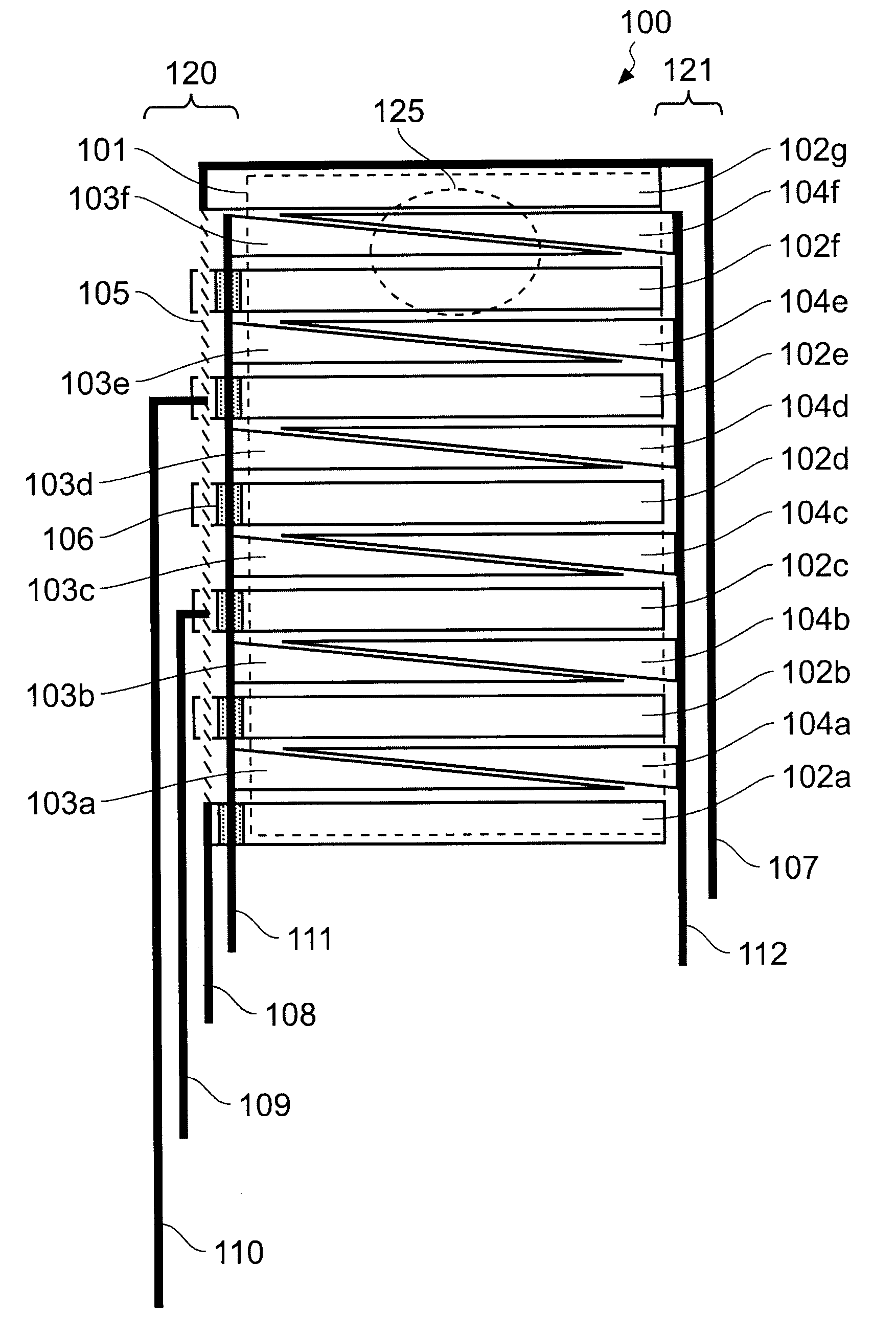
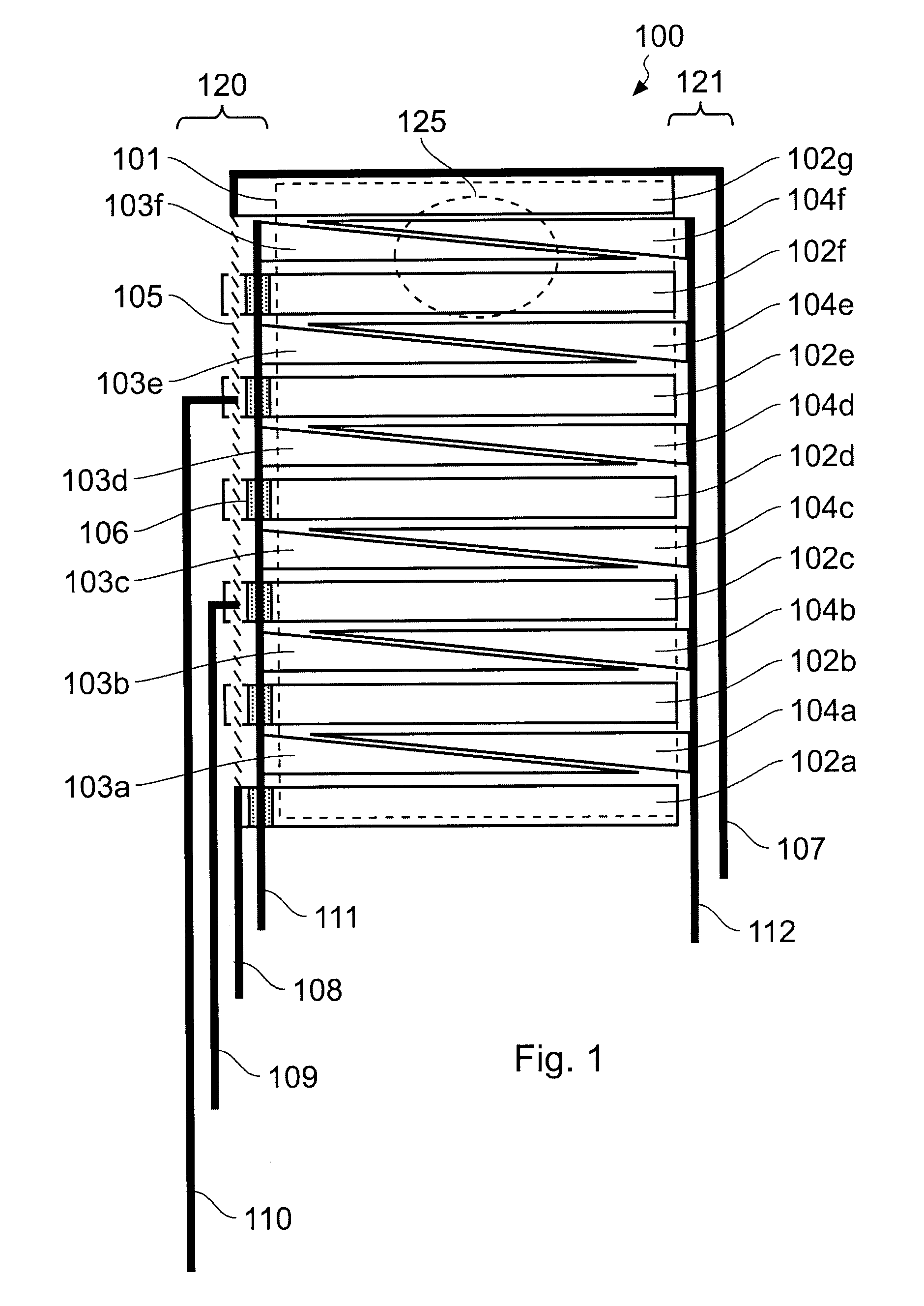
[0049]Referring to the drawings, in FIG. 1 there is shown the invention. FIG. 1 shows in plan view a capacitive touch sensing array 100 having a usable touch area 101 (shown as a dotted outline). Electrodes 102a-g resolve a first axis (shown as y), while electrodes 103a-f and 104a-f resolve a second axis (shown as x). In practice the configuration is reversible with respect to x and y in some applications. The x axis is resolved by the field gradients produced by the triangular shapes as is known in the art. Left-side and right-side connections 111 and 112 respectively are wired to a circuit (not shown) which senses the capacitive loading on these electrodes and obtains a ratiometric measurement of touch location along the x axis.

[0050]The y axis is resolved by the use of a resistive element 105 which runs along one side of the electrodes and which connects to electrodes 102a-g. The field gradient on this axis is produced by 105 in a manner known according to my co-pending U.S. appl...

second embodiment

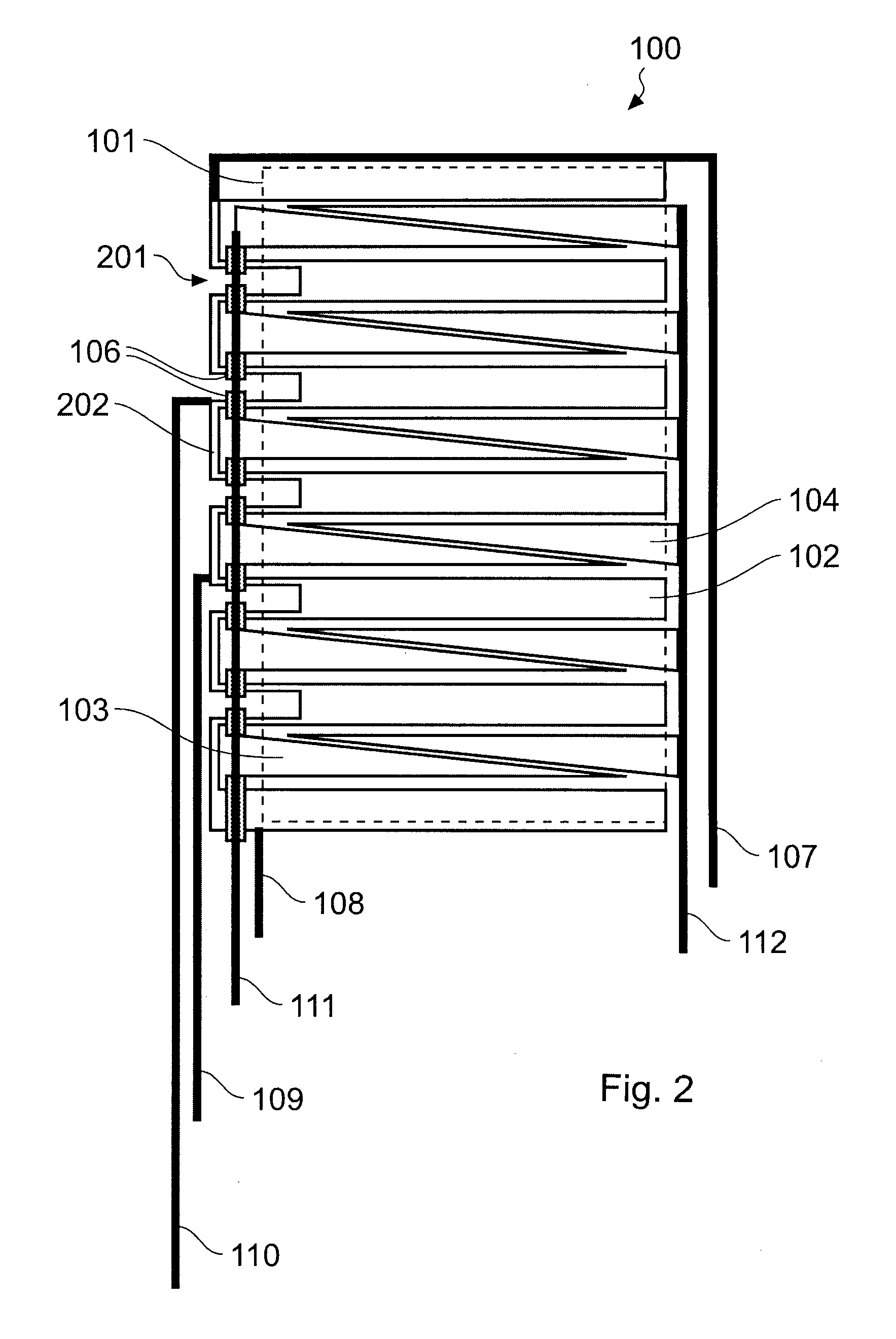
[0056]Turning now to FIG. 2, there is shown a second embodiment with a slightly different configuration of the electrode array 100. In this configuration, the resistive strip 105 is replaced by the same conductive material as used in the electrodes. In the case of ITO, a common value of sheet resistance is 300 ohms per square. In order to use the ITO itself as a resistive element, to achieve the relatively high values of end-to-end resistance required, the path length must be increased in some manner. In FIG. 2 this is achieved by using the bars 102 as an additional path for the current to flow, by means of cutouts 201 within the bars. Bar-to-bar traces 202 are also made of the electrode material so that the entire structure composed of electrodes 102, 103, 104 and traces 202 are made in one step on the same layer. Dielectric 106 separates the electrode conductor from the left x connection 111 to prevent short circuits.

third embodiment

[0057]Turning now to FIG. 3, there is shown a third embodiment with yet another configuration of electrode array 100, whereby the required resistive strip shown as 105 in FIG. 1 is incorporated into the y resolving bars 102 themselves. The path for the resistance is serpentine from top to bottom (as shown) with resistive routing 202 connecting each bar to the next. The end bars 310, 311 at the top and bottom of the electrode pattern do not participate in the resistive path; as a result they are equipotential with respect to their connecting wires 107 and 108. Since the right x connection 112 still needs to connect to the right triangles 104, additional thin crossover dielectric 301 is required between each of ones 104 and 112.

[0058]Dotted outlines 320 and 325 show the areas of finger contact and hand shadow respectively which will be discussed further below.

[0059]FIG. 4 shows an ACE capable circuit 400 for operating the touch screen electrode set 100. As shown, there are six sensing...


PUM


Abstract

A capacitive two-dimensional (2D) touch panel has three sets of interleaved electrodes. A first set of electrodes is spaced apart along the y-direction and these are galvanically connected to each other by a resistive strip connected at either end to a connection line. A second set of electrodes is also arrayed along the y-direction and these are galvanically connected to each other via a notionally non-resistive first connection. A third set of electrodes is also arrayed along the y-direction and these are galvanically connected to each other via a notionally non-resistive second connection. The second and third sets of electrodes are interleaved without galvanic cross-conduction to provide a gradient along the x-direction to resolve touch position in the x-direction. The first set of electrodes resolves touch position along the y-direction. Passive or active capacitive sensing techniques may be used to acquire the position information from the 2D touch panel.

Description

BACKGROUND OF THE INVENTION[0001]The invention pertains to 2-dimensional touch sensing surfaces operable by a human finger, or a stylus. Example devices include touch screens and touch pads, particularly those over LCDs, CRTs and other types of displays, or pen-input tablets, or encoders used in machinery for feedback control purposes. In particular this invention pertains to 2-dimensional capacitive touch sensing surfaces constructed so that the sensing layer is disposed on the rear of a panel or lens surface, particularly for use in smaller touch screens where there is a space constraint along the edges of the screen, for example in portable devices such as mobile phones or handheld media players. In addition the invention addresses the need to reduce the effects of capacitive ‘hand shadow’.[0002]In my earlier co-pending U.S. application Ser. No. 10 / 916,759 (published as US2005 / 0041018A), there is a pattern of galvanically coupled conductors which have anisotropic galvanic propert...

Claims


Application Information

Patent Timeline
Patent Type & Authority Applications(United States)
IPC IPC(8): G06F3/041
CPCG06F3/044G06F3/0443H03K17/955H03K17/9622G06F3/0448G06F3/045
Inventor PHILIPP, HARALD
Owner ATMEL CORP
Why Eureka
Try Eureka