Liquid-Crystal Panel, Manufacturing Process Therefor and Electronic Device Equipped with Liquid-Crystal Panel

a technology of liquid crystal panel and manufacturing process, which is applied in the direction of instruments, non-linear optics, optics, etc., can solve the problems of obscuring image in dark places, power consumption increase, and dazzling indoor images, so as to reduce the intensity of backlight, improve light efficiency, and display in bright places.

Inactive Publication Date: 2007-11-08
NEC CORP +9
View PDF5 Cites 21 Cited by
  • Summary
  • Abstract
  • Description
  • Claims
  • Application Information

AI Technical Summary

Benefits of technology

[0064] According to this invention, in contrast to a conventional semi-transmissive liquid-crystal panel, an outside light can be completely reflected and a backlight can be completely transmitted without any restrictions to reflection of an outside light or transmission of a backlight beam. Although there are practically some problems in terms of, for example, a reflection efficiency of a reflection film and a film transmittance, theoretically an outside light can be 100% reflected in a bright place to allow the device to operate as a reflective liquid-crystal panel and a backlight can be 100% transmitted in a dark place to allow the device to operate as a transmissive liquid-crystal panel.
[0065] As a result, in comparison with a conventional semi-transmissive liquid-crystal panel, a light efficiency is increased and display in a bright place is clearer. Thus, the device can be operated as a reflection type liquid-crystal panel in a darker place compared to a conventional device and an intensity of a backlight can be reduced in a dark place.
[0066] According to this invention, a backlight can be OFF under wider conditions. Thus, a period for which a backlight is OFF can be reduced and a backlight illumination can be reduced, so that a power consumption can be reduced and, in a mobile device driven by a battery, a battery life can be increased.

Problems solved by technology

However, image contrast is deteriorated in an outdoor area which is brighter than emission intensity of natural light, leading to an obscure image.
When a light source is intensified for preventing contrast deterioration outside, dazzling occurs in an indoor image and power consumption is increased.
In contrast, a reflective liquid crystal display has an advantage of higher outdoor visibility because it reflects an outside light to display an image, but has a drawback that an image is obscure in a dark place.
Although the problem can be improved by incorporating a front light, a front light has a drawback that it cannot evenly illuminate the whole display.
However, an image in a semi-transmissive liquid crystal display is inferior to that in a transmissive liquid crystal display or organic EL display in a dark place and inferior to that in a reflective liquid crystal display in a bright place.
Robustness leads to a thinner panel.
A conventional transmissive / semi-transmissive liquid crystal display is thick and heavy because it uses a backlight.
However, these liquid-crystal panels are transparent, which are not manufactured, taking into account the use under various illumination conditions, e. g., a cell phone which may be used during moving from a dark place to a bright place.

Method used


Image

  • Liquid-Crystal Panel, Manufacturing Process Therefor and Electronic Device Equipped with Liquid-Crystal Panel
  • Liquid-Crystal Panel, Manufacturing Process Therefor and Electronic Device Equipped with Liquid-Crystal Panel
  • Liquid-Crystal Panel, Manufacturing Process Therefor and Electronic Device Equipped with Liquid-Crystal Panel

Examples


Embodiment Construction

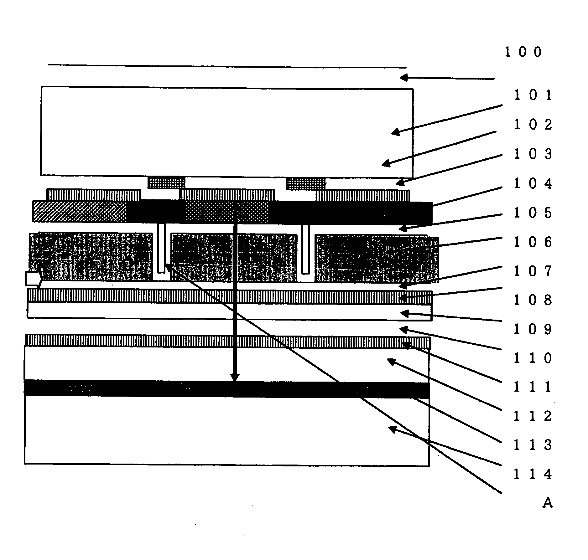
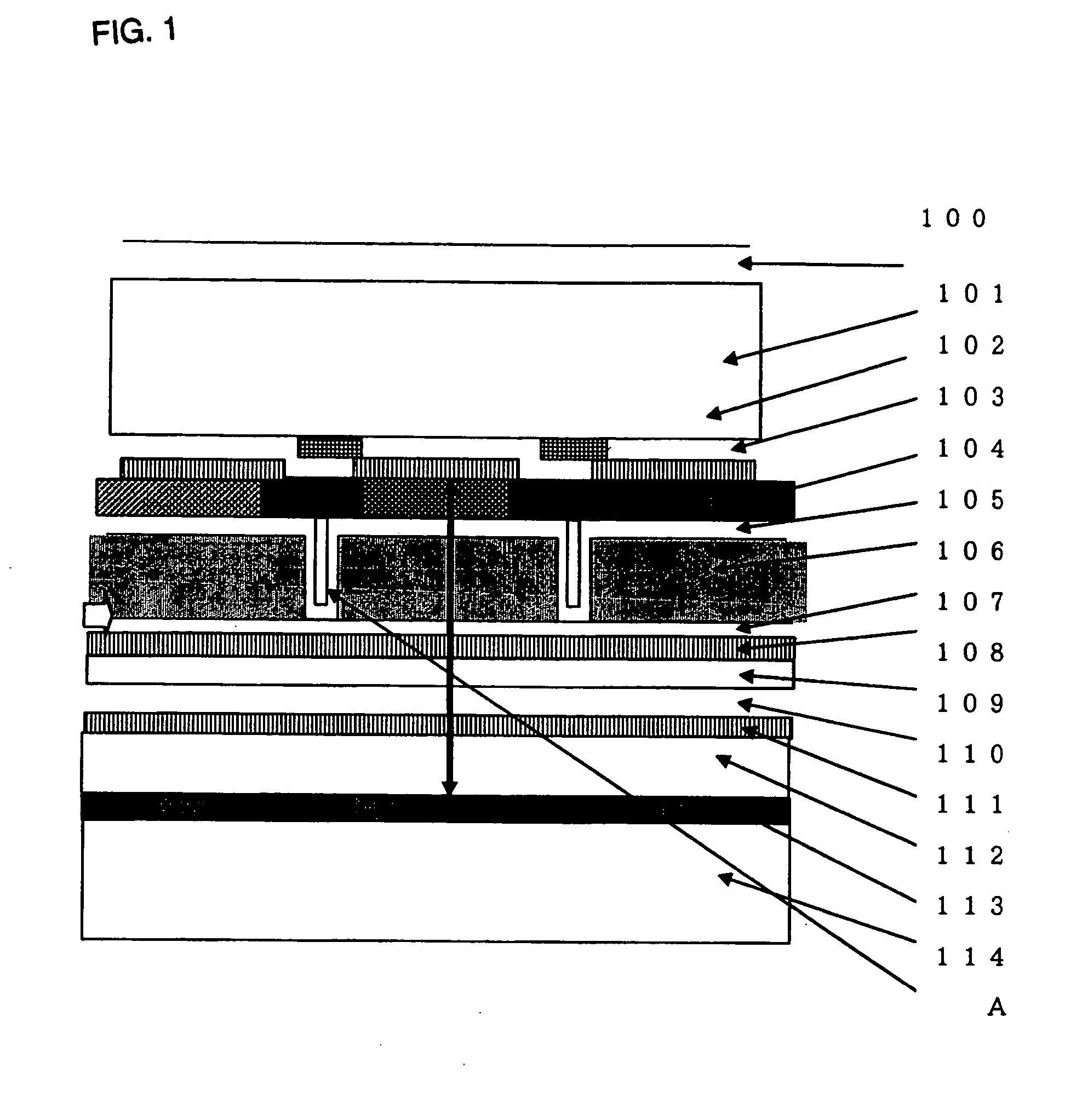
[0077] A first embodiment of this invention will be described with reference to a schematic view in FIG. 1. FIG. 1 is a cross-sectional view of a liquid crystal display panel with a backlight of this first embodiment.

[0078] By a known method, on a silicon film formed on a first glass substrate 101 are formed a thin-film transistor, an interconnection 102, a color filter 104, then a pixel electrode 103 as a transparent electrode and finally an oriented film 105.

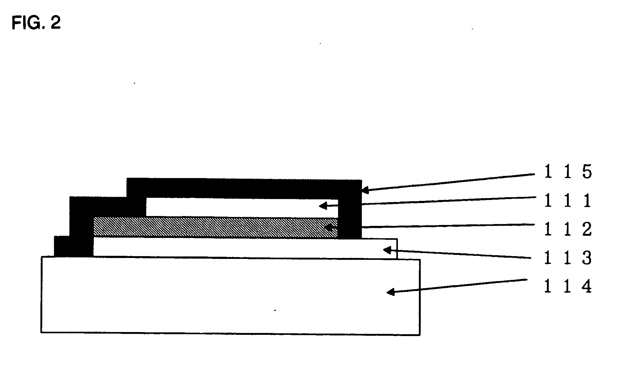
[0079] On a second glass substrate 114 are formed a reflection electrode 113, an organic EL layer 112 to be a light-emitting layer in a thin-film light emitting device, a transparent electrode 111, a polarizing film 110, a retardation film 109, a counter electrode 108 as a transparent electrode for a liquid crystal, and an orienting plate 107. The liquid crystal 106 is sandwiched between the orienting plate film 105 and the oriented film 107. A spacer A is for ensuring a distance between the oriented film 105 and the oriente...


PUM

PropertyMeasurementUnit
transmittanceaaaaaaaaaa
distanceaaaaaaaaaa

Abstract

A semi-transmissive liquid-crystal panel is a useful mobile display device which can provide a clear image in both dark and bright places. However, there has been needed a light-weighted and highly durable display device with a lower power consumption, pursing advantages of a single transparent/reflection type liquid-crystal panel. According to this invention, there is provided a liquid crystal display panel comprising a rear-emitting light source, comprising a liquid crystal device formed on a first substrate in which a liquid crystal layer is sandwiched between a transparent first electrode and a transparent second electrode which at least face each other and a rear-emitting light source for the liquid crystal device formed on a second substrate in which a thin-film flat light emitting device is sandwiched between an optically opaque third electrode and a transparent fourth electrode which at least face each other, wherein the third electrode is a reflection film disposed in the side of the second substrate, which reflects an outside light entering via the liquid crystal layer into the liquid crystal layer; and the fourth electrode is disposed facing the second electrode, and the insulating film sandwiched between the fourth electrode and the second electrode is a film continuously formed on the fourth electrode.

Description

TECHNICAL FIELD [0001] This invention relates to a liquid-crystal panel, a manufacturing process therefor and an electronic device equipped with a liquid-crystal panel. BACKGROUND ART [0002] As an information society has been recently developed, a conventional CRT (Cathode Ray Tube) display conventionally used as an imaging apparatus in an information device has been replaced by a flat display due to its larger size. [0003] Application of information devices have been expanded from indoor stationary types to mobile types. In contrast to stationary types, mobile type information devices are used in various situations. [0004] Known flat displays include a plasma display, a liquid crystal display and an organic EL display (Organic Light Emitted Display). A plasma display is not suitable for a mobile device because it requires a high voltage from its operation principle, while a liquid crystal display and an organic EL display which can be operated with low power consumption are suitabl...

Claims


Application Information

Patent Timeline
Patent Type & Authority Applications(United States)
IPC IPC(8): G02F1/13357G02F1/1335H01L51/50H05B33/04H05B33/14
CPCG02F1/133555G02F1/133603H10K59/50H10K50/844G02F1/1335
Inventor TAKECHI, KAZUSHIGESUMIYOSHI, KENFUJIEDA, ICHIROTAKAHASHI, TATSUMIGENDA, KAZUOKUMANO, ATSUSHIOSHIMA, NOBORUMATSUOKA, YOSHIKIEGUCHI, TOSHIMASAYAMAOKA, SHIGENORIONO, YOSHIYUKIYONEHARA, HISATOMOSUZUKI, MOTOYUKITSUKUDA, AKIMITSUSEKINE, NORMASATSURUOKA, YASUO
Owner NEC CORP
Why Eureka
Try Eureka