Method for forming high-resolution pattern having desired thickness or high aspect ratio using dry film resist

Inactive Publication Date: 2007-11-08
KOREA INST OF MASCH & MATERIALS
View PDF13 Cites 28 Cited by
  • Summary
  • Abstract
  • Description
  • Claims
  • Application Information

AI Technical Summary

Benefits of technology

[0011]The present invention has been made to solve the above-described problems occurring in the art, and it is an object of the present invention to achieve a high-resolution pattern by exposing a dry film resist to light either by irradiating a focusable energy beam directly and selectively onto the dry film resist attached onto a substrate or by projecting a specific wavelength range of light onto the dry film resist through a mask or a diffractive optical element, removing the exposed region through a development process, and depositing a functional material into the region from which the dry film resist was removed. Another object of the present invention is to obtain a desired pattern thickness by setting the thickness of an initial dry film resist to be sufficient in view of a reduction in thickness resulting from the drying of ink, and charging ink into the selected thickness of the film. Still another object of the present invention is to provide a s

Problems solved by technology

However, this photolithography method has problems in that a large amount of material is wasted and a process is complicated, leading to a reduction in efficiency.
Also, because a large-area mask is used, it is difficult to implement a new design in a short time.
Also, in a thick film process of depositing a functional material for patterns to a thickness of the micrometer scale or larger using a process such as sputtering or CVD in a short time, photolithography is unsuitable in terms of process efficiency.
When such an inkjet is used to form a pattern, there is a problem in that an undesired excessive decrease in thickness occurs depending on the composition of ink, and this phenomenon is shown in FIG. 1a. Also, to form the pattern so that it has high re

Method used


Image

  • Method for forming high-resolution pattern having desired thickness or high aspect ratio using dry film resist
  • Method for forming high-resolution pattern having desired thickness or high aspect ratio using dry film resist
  • Method for forming high-resolution pattern having desired thickness or high aspect ratio using dry film resist

Examples


Embodiment Construction

[0018]Hereinafter, the present invention will be described in further detail with reference to the accompanying drawings.

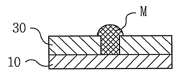
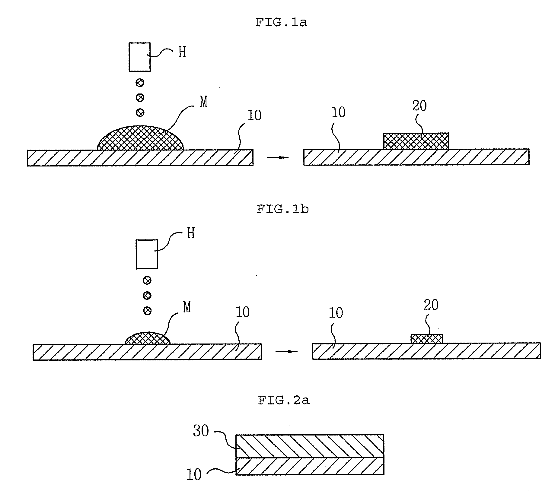
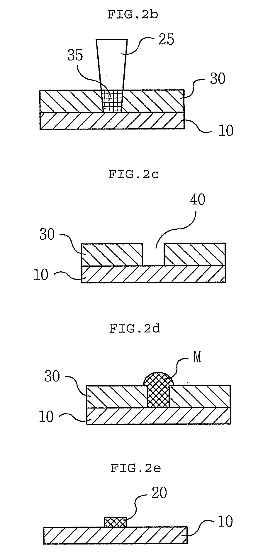
[0019]As described above, the present invention provides a method for forming a high-resolution pattern, which can achieve a precise pattern linewidth and thickness by reducing width and, at the same time, maintaining a given height, the method comprising: exposing to light a dry film resist attached onto the substrate either by irradiating a focusable energy beam selectively and directly onto the dry film resist or by projecting a specific wavelength range of light onto the dry film resist through a mask or a diffractive optical element; removing the dry film resist from the exposed region to be deposited with a functional material, through a development process; and depositing the functional material into the region from which the dry film resist was removed. For this purpose, the inventive method comprises: an attachment step of attaching a dry film resist onto...


PUM


Abstract

Disclosed herein is a method for forming a pattern, comprising: attaching a single-layer or multi-layer dry film resist made of a semi-solid or solid material to part or all of the surface of a substrate; exposing the dry film resist to light either by irradiating a focusable energy beam directly onto the resist or by projecting a specific wavelength range of light onto the resist, to form a region to be filled with a functional material; charging the functional material into the formed region using a method such as inkjetting; drying the functional material; and removing the dry film resist, thus obtaining the desired pattern.

Description

BACKGROUND OF THE INVENTION[0001]1. Field of the Invention[0002]The present invention relates to a method for forming a high-resolution pattern, and more particularly to a method for forming a high-resolution pattern having a high aspect ratio, comprising the steps of: an attachment step of attaching a dry film resist onto a substrate; an exposure step of exposing a dry film resist to light either by irradiating a focusable energy beam directly onto the dry film resist without using a mask or a diffractive optical element, or by projecting a specific wavelength range of light onto the dry film resist through a mask or a diffractive optical element, to pattern the dry film resist into the desired shape, thus forming a pattern; a pattern template-forming step of removing the exposed region using a development process; and a deposition step of depositing a functional material into the region from which the dry film resist was removed.[0003]2. Description of the Prior Art[0004]Generally...

Claims


Application Information

Patent Timeline
IPC IPC(8): G03F7/26
CPCG03F7/40H05K3/125H05K2203/1173H05K2203/013H05K2203/0568H05K3/1258H10K71/611
Inventor SHIN, DONG-YOUNKIMYUN, SO-NAMHAM, YOUNG-BOGCHOI, BYUNG-OH
Owner KOREA INST OF MASCH & MATERIALS
Why Eureka
Try Eureka