Semiconductor device having MIS structure and its manufacture method

a technology of semiconductor devices and manufacturing methods, applied in semiconductor devices, basic electric elements, electrical equipment, etc., can solve the problems of increasing the possibility of gate leakage current, and achieve the effect of suppressing damages and sufficient mechanical strength of the gate electrod

Active Publication Date: 2007-11-22
FUJITSU LTD
View PDF22 Cites 42 Cited by
  • Summary
  • Abstract
  • Description
  • Claims
  • Application Information

AI Technical Summary

Benefits of technology

[0038] Since the gate electrode is supported by the lower protective film and upper protective film, it is possible to retain a sufficient mechanical strength of the gate electrode. Since lower protective film is wet etched, it is possible to suppress damages to be introduced into the gate insulating film under the gate electrode.BRIEF DESCRIPTION OF THE DRAWINGS

Problems solved by technology

However, as the gate-channel distance is shortened, a problem of an increase in gate leakage current is likely to occur.

Method used


Image

  • Semiconductor device having MIS structure and its manufacture method
  • Semiconductor device having MIS structure and its manufacture method
  • Semiconductor device having MIS structure and its manufacture method

Examples


Embodiment Construction

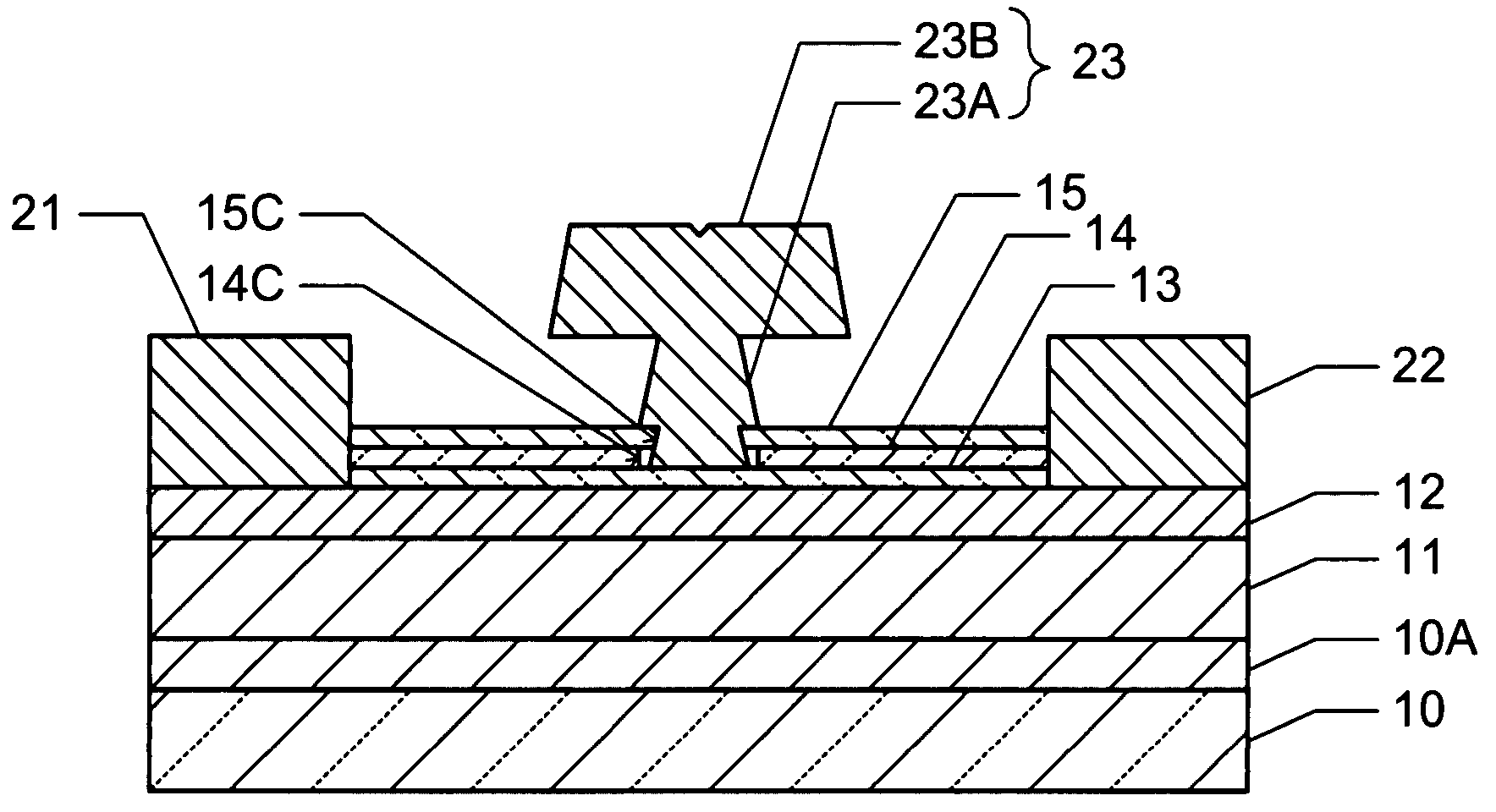
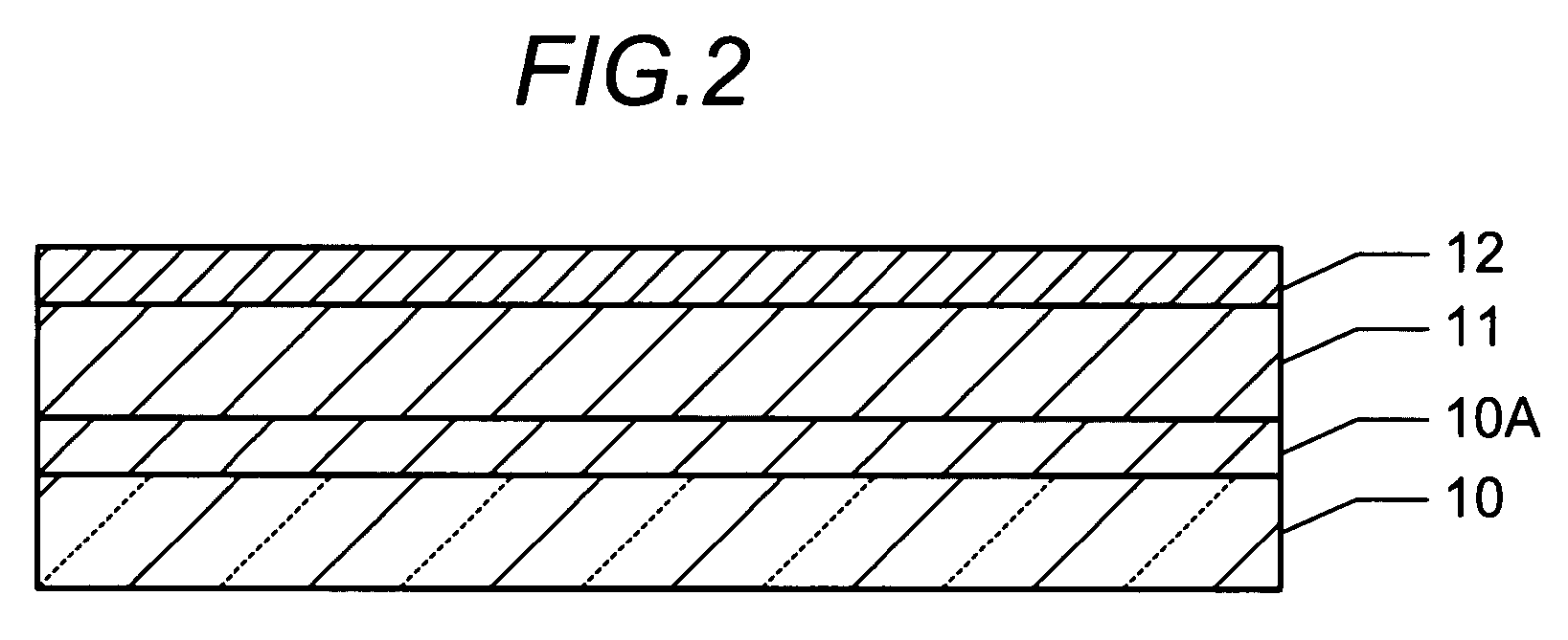
[0056]FIG. 1 is a cross sectional view of a semiconductor device according to an embodiment. On a substrate 10 made of sapphire (Al2O3) or silicon carbide (SiC), a buffer layer 10A made of undoped GaN is formed. On the buffer layer 10A, a channel layer (electron transit layer) 11 made of undoped GaN and a barrier layer (electron supply layer) 12 made of undoped or n-type impurity doped AlGaN are stacked in this order.

[0057] A source electrode 21 and a drain electrode 22 are formed on the barrier layer 12, keeping a distance from each other. The source electrode 21 and drain electrode 22 are electrically connected to the channel layer 11. A gate insulating film 13 made of SiN is formed on the barrier layer 12 between the source electrode 21 and drain electrode 22. On the gate insulating film 13, a lower protective film 14 made of SiO2 and an upper protective film 15 made of SiN are stacked.

[0058] An opening 15C is formed through the upper protective film 15, and an opening 14C is f...


PUM


Abstract

A channel layer (11) made of compound semiconductor and a barrier layer (12) made of compound semiconductor having a band gap wider than the channel layer are formed over a substrate. A gate insulating film (13) made of first insulating material is formed on the barrier layer over the channel region. A gate electrode (23) is formed on a partial area of the gate insulating film. A protective film is disposed on the gate insulating film on both sides of the gate electrode. The protective film comprises a lower protective film (14) made of second insulating material whose etching resistance is different from the first insulating material and an upper protective film (15) made of third insulating film whose etching resistance is different from the second insulating material. A source electrode and a drain electrode are electrically connected to the channel layer on both sides of the gate electrode.

Description

TECHNICAL FIELD [0001] The present invention relates to a semiconductor device having a MIS structure and its manufacture method, and more particularly to a semiconductor device applicable to a high electron mobility transistor (HEMT) which is a high frequency device particularly used for communications and its manufacture method. BACKGROUND ART [0002] Research and development about a GaN based HEMT has been conducted mainly as transistors capable of high power and high voltage operations. In addition, it has been theoretically predicted that the GaN based HEMT holds the potential that the operation speed can be higher. The most straightforward approach to make higher the operation speed of an FET such as HEMT is to shorten a gate length. [0003] From the viewpoint of scaling rules of HEMT, as the gate length is shortened, a gate-channel distance is required to be shortened. However, as the gate-channel distance is shortened, a problem of an increase in gate leakage current is likely...

Claims


Application Information

Patent Timeline
Patent Type & Authority Applications(United States)
IPC IPC(8): H01L29/739H01L21/3205
CPCH01L29/66462H01L29/7787H01L29/7786
Inventor ENDOH, AKIRAYAMASHITA, YOSHIMI
Owner FUJITSU LTD
Why Eureka
Try Eureka