

Field-effect transistor
a field-effect transistor and transistor technology, applied in the field of field-effect transistors, can solve the problems of increased chip area and high cost, difficult to realize normal off characteristics, and increased deterioration of power switching elements
- Summary
- Abstract
- Description
- Claims
- Application Information
AI Technical Summary
Benefits of technology
Problems solved by technology
Method used
Image

Examples
embodiment 1
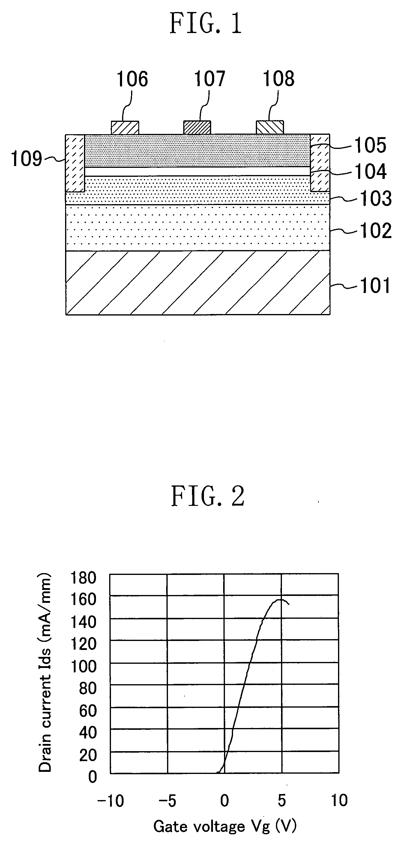
[0058]FIG. 1 is a cross section of a heterojunction field-effect transistor of Embodiment 1 of the present invention. In FIG. 1 illustrated are a sapphire substrate 101, an AlN buffer layer 102, an AlGaN liner layer 103, a GaN channel layer 104, an AlGaN electron supply layer 105, a Ti / Al source electrode 106, a PdSi gate electrode 107, a Ti / Al drain electrode 108, and a device isolation layer 109.
[0059]As shown in FIG. 1, on a (0001) plane of the sapphire substrate 101, the AlN buffer layer 102 having a thickness of 500 nm, the AlGaN liner layer 103 which is formed of Al0.05Ga0.95N and has a thickness of 0.5 μm, the GaN channel layer 104 having a thickness of 10 nm, and the electron supply layer 105 which is formed of A10.15Ga0.85N and has a thickness of 25 nm are provided in this order by Metal Organic Chemical Vapor Deposition (MOCVD). On a surface of the AlGaN electron supply layer 105, the PdSi gate electrode 107, the Ti / Al source electrode 106, and the Ti / Al drain electrode 10...
embodiment 2
[0083]FIG. 8 is a cross section illustrating a heterojunction field-effect transistor of Embodiment 2 of the present invention. In FIG. 8 illustrated are a Si substrate 701, an AlN buffer layer 702, an AlGaN buffer layer 703, an AlN / GaN periodic structure 704, an AlGaN liner layer 705, a GaN channel layer 706, an AlGaN electron supply layer 707, a Ti / Al source electrode 708, a PdSi gate electrode 709, a Ti / Al drain electrode 710, and a device isolation layer 711.
[0084]As shown in FIG. 8, on a (111) plane of the Si substrate701, the AlN buffer layer 701 (film thickness: 40 nm), the buffer layer 703 (Al0.26Ga0.74N, film thickness: 40 nm), the AlN / GaN periodic structure 704 (total film thickness: 0.5 μm), the liner layer 705 (Al0.05Ga0.95N, film thickness: 0.5 μm), the GaN channel layer 706 (film thickness: 10 nm), and the AlGaN electron supply layer 707 (Al0.15Ga0.85N, film thickness: 25 nm) are formed in this order by MOCVD. On a surface of the AlGaN electron supply layer 707, the Pd...
embodiment 3
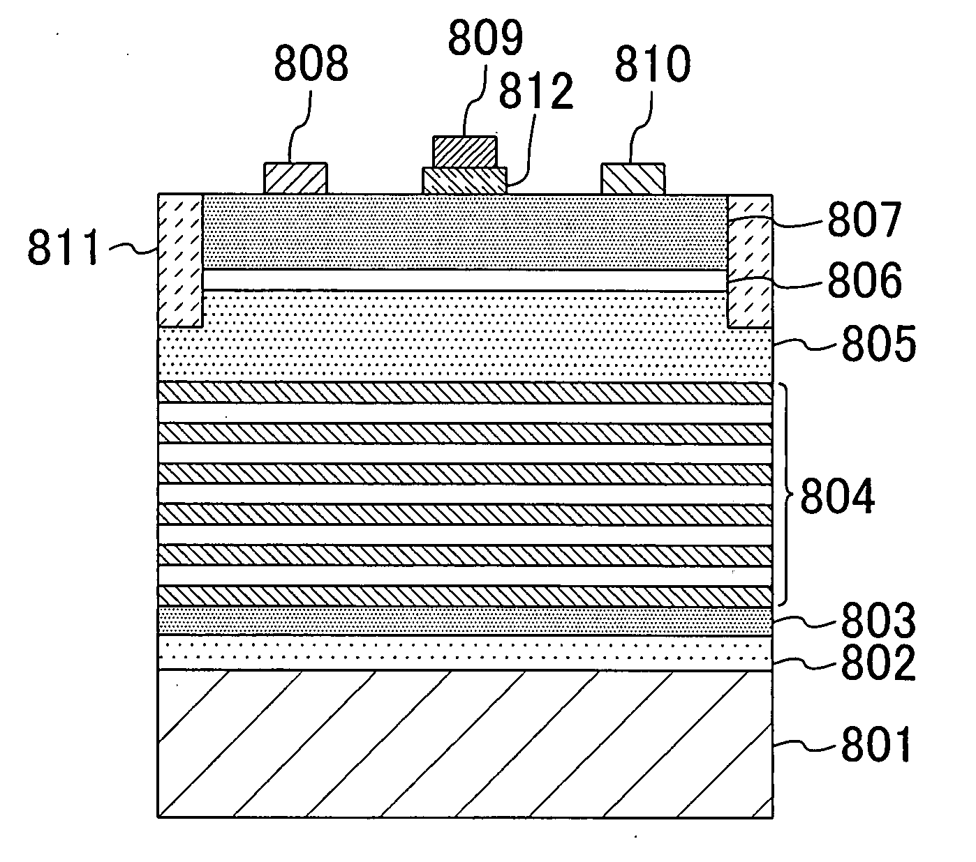
[0088]FIG. 9 is a cross section illustrating a heterojunction field-effect transistor of Embodiment 3 of the present invention. In FIG. 9 illustrated are a Si substrate 801, an AlN buffer layer 802, an AlGaN buffer layer 803, an AlN / GaN periodic structure 804, an AlGaN liner layer 805, a GaN channel layer 806, an AlGaN electron supply layer 807, a Ti / Al source electrode 808, a PdSi gate electrode 809, a Ti / Al drain electrode 810, a device isolation layer 811, and a p-type GaN layer 812.
[0089]As shown in FIG. 9, on a (111) plane of the Si substrate 801, the AlN buffer layer 802 (film thickness: 40 nm), the AlGaN buffer layer (Al0.26Ga0.74N, film thickness: 40 nm), the AlN / GaN periodic structure 804 (total film thickness: 0.5 μm), the AlGaN liner layer (Al0.05Ga0.95N, film thickness: 0.5 μm), the GaN channel layer 806 (film thickness: 10 nm), the AlGaN electron supply layer 807 (Al0.2Ga0.8N, film thickness: 25 nm), and the p-type GaN layer 812 (film thickness: 200 nm) are formed in th...
PUM
 Abstract
Description
Claims
Application Information