Gallium nitride material devices and associated methods

a technology of gallium nitride and material, applied in the direction of semiconductor devices, basic electric elements, electrical apparatus, etc., can solve the problems of difficult to grow high-quality gallium nitride materials on certain substrates, difficult to form gallium nitride material devices meeting the property requirements of certain applications, and applications for rf power transistors may have particularly demanding property requirements

Active Publication Date: 2007-11-29
MACOM TECH SOLUTIONS HLDG INC
View PDF93 Cites 37 Cited by
  • Summary
  • Abstract
  • Description
  • Claims
  • Application Information

AI Technical Summary

Benefits of technology

[0009] In another aspect, a method of operating a transistor is provided. The method comprises operating a transistor comprising gallium nitride material at a power density of at least 10 W/mm and a drain efficiency of at least 70%.
[0010] In another aspect, a method of operating a transistor is provided. The method comprises operating a transistor comprising gallium nitride material at a

Problems solved by technology

Despite the attractive properties noted above, a number of challenges exist in connection with developing gallium nitride material-based devices.
For example, it may be difficult to grow high quality gallium nitride materials on certain substrates, particularly silicon, due to property differences (e.g., lattice constant a

Method used


Image

  • Gallium nitride material devices and associated methods
  • Gallium nitride material devices and associated methods
  • Gallium nitride material devices and associated methods

Examples


example 1

[0120] This example describes production and characterization of gallium nitride material transistors having a source field plate, as well as comparison to gallium nitride material transistors without a source field plate.

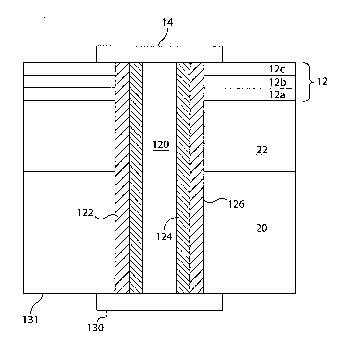
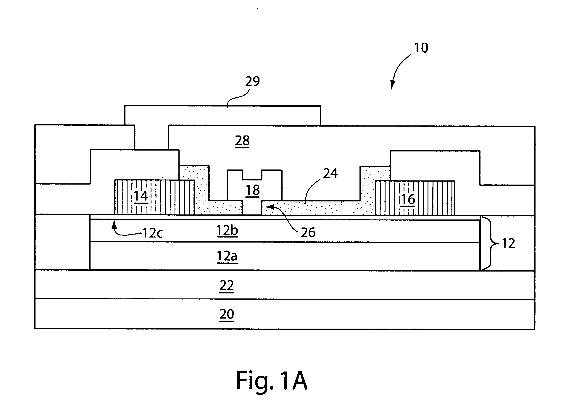
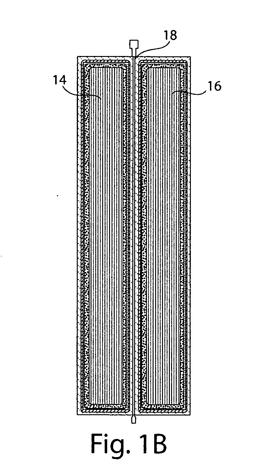
[0121] Gallium nitride material regions including an undoped Al0.26Ga0.74N layer formed on a GaN layer were grown on high resistivity Si (111) substrates by metal organic chemical vapor deposition (MOCVD). The structures included a compositionally-graded AlGaN transition layer formed between the substrate and the gallium nitride material region. The aluminum concentration in the transition layer decreased in a step-wise manner in a direction from the substrate to the gallium nitride material region. The structures were further processed to produce HFET devices having a similar layer structure as the device shown in FIG. 1A. The devices had a gate length of 0.7 μm, gate-to-source spacing of 1 μm, and gate-to-drain spacing of 3 μm. The single chip transistors had a ...


PUM


Abstract

Gallium nitride material devices and methods associated with the same. In some embodiments, the devices may be transistors which include a conductive structure connected to a source electrode. The conductive structure may form a source field plate which can be formed over a dielectric material and can extend in the direction of the gate electrode of the transistor. The source field plate may reduce the electrical field (e.g., peak electrical field and/or integrated electrical field) in the region of the device between the gate electrode and the drain electrode which can lead to a number of advantages including reduced gate-drain feedback capacitance, reduced surface electron concentration, increased breakdown voltage, and improved device reliability. These advantages enable the gallium nitride material transistors to operate at high drain efficiencies and/or high output powers. The devices can be used in RF power applications, amongst others.

Description

RELATED APPLICATIONS [0001] This application claims priority to U.S. Provisional Patent Application Ser. No. 60 / 741,608, filed Dec. 2, 2005, which is incorporated herein by reference.FIELD OF INVENTION [0002] The invention relates generally to gallium nitride material devices and, more particularly, to gallium nitride material devices that include a source field plate and methods associated with the same. BACKGROUND OF INVENTION [0003] Gallium nitride materials include gallium nitride (GaN) and its alloys such as aluminum gallium nitride (AlGaN), indium gallium nitride (InGaN), and aluminum indium gallium nitride (AlInGaN). These materials are semiconductor compounds that have a relatively wide, direct bandgap which permits highly energetic electronic transitions to occur. Gallium nitride materials have a number of attractive properties including high electron mobility, the ability to efficiently emit blue light, and the ability to transmit signals at high frequency, amongst others....

Claims


Application Information

Patent Timeline
IPC IPC(8): H01L29/78H01L21/336
CPCH01L29/2003H01L29/402H01L29/7787H01L29/42316H01L29/41725H01L29/66462
Inventor JOHNSON, JERRY WAYNESINGHAL, SAMEERHANSON, ALLEN W.THERRIEN, ROBERT JOSEPH
Owner MACOM TECH SOLUTIONS HLDG INC
Why Eureka
Try Eureka