Power Amplifier with Stabilising Network

a power amplifier and network technology, applied in the direction of amplifier modifications to reduce non-linear distortion, high frequency amplifiers, amplitude modulation details, etc., can solve the problems of affecting the output stage, and presenting a power amplifier impedance to the modulable supply, so as to achieve the effect of dilating the series resonan

Active Publication Date: 2007-11-29
SNAPTRACK
View PDF13 Cites 57 Cited by
  • Summary
  • Abstract
  • Description
  • Claims
  • Application Information

AI Technical Summary

Benefits of technology

[0016] A series resonance at the power supply is equivalent to a parallel resistance at the junction between the inductance and the capacitance. This junction is the drain of the transistor. The low impedance at the power supply terminal is equivalent to a high impedance at the transistor terminal. This provides a solution of presenting a low impedance to the transistor terminal to thereby damp out the series resonance appearing at the power supply terminal.

Problems solved by technology

However, in such an arrangement the power amplifier presents an impedance to the modulatable supply.
In particular, this impedance can change rapidly with frequency due to a presence of a high Q series resonance, making accurate high bandwidth modulation very difficult.
This series resonance presents problems if the supply modulation is to be applied at high bandwidths.
However it is difficult to achieve this without compromising the output stage with respect to some other parameter.
This could potentially have a major implication on the cost of such units, as well as the ability to manufacture such units.
This could compromise the RF stage efficiency, gain or bandwidth.
Thus a problem exists with current power amplifier output stages in that at high frequencies a series resonance is presented at the power supply terminal of the amplifier as a consequence of the output capacitance of the transistor forming a high Q resonant network with the supply feed inductance.
This network creates a source of potential instability, and creates a long time constant energy storage means that contributes to memory effect, and renders any form of wideband envelope modulation difficult to apply.

Method used


Image

  • Power Amplifier with Stabilising Network
  • Power Amplifier with Stabilising Network
  • Power Amplifier with Stabilising Network

Examples


Embodiment Construction

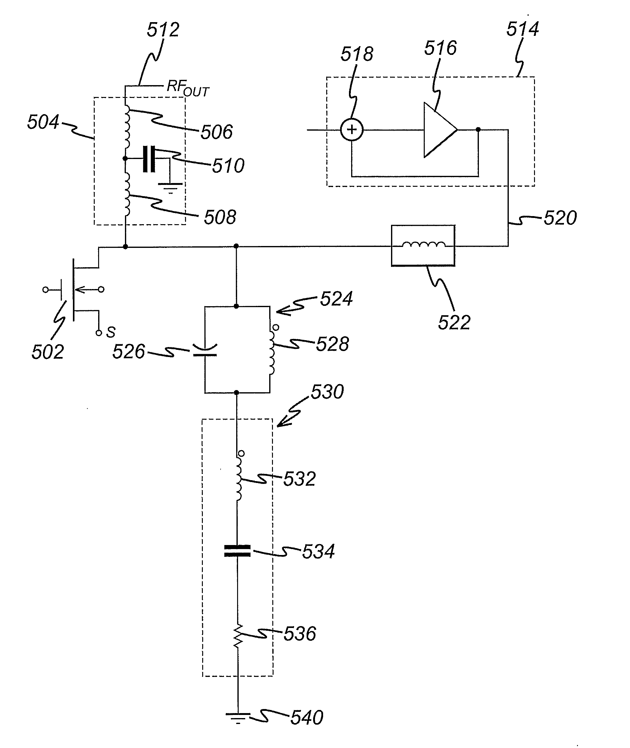
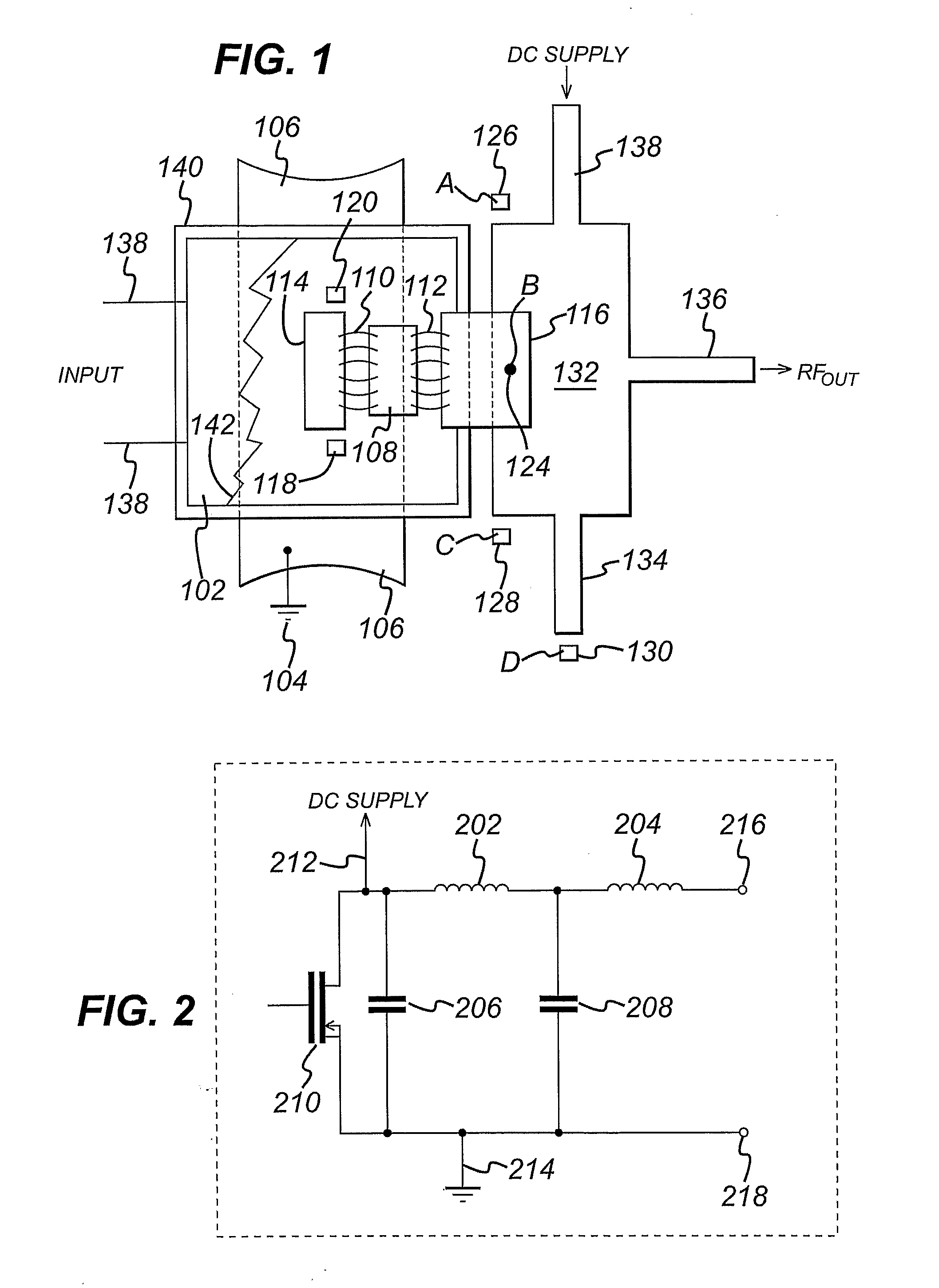
[0023] With reference to FIG. 1, an example physical representation of a RF power stage with which embodiments of the invention is implemented is illustrated.

[0024] With reference to FIG. 1, reference numeral 140 generally represents a transistor package. Reference numeral 102 generally represents the top surface of the transistor package. The jagged line 142 represents the opening of the top surface of the transistor package to show at least part of the internal structure thereof. The internal structure of the transistor package includes an array of transistor power amplifiers 114 and a corresponding array or bank of matching capacitors 108. The plurality of transistor power amplifiers 114 are connected to the corresponding plurality of capacitors 108 via a plurality of bond wires 110. The plurality of capacitors 108 are connected, via a further plurality of bond wires 112, to a metallisation 116 which represents the connection of the bond wires 112 external to the transistor pack...


PUM

PropertyMeasurementUnit
impedanceaaaaaaaaaa
impedanceaaaaaaaaaa
inductanceaaaaaaaaaa

Abstract

A power amplifier circuit comprising a transistor for receiving a signal to be amplified at an input and for outputting an amplified signal at an output; a modulated power supply connected to the transistor output; and a resistive element connected at the transistor output such that a low impedance is maintained at the transistor output across a range of operational frequencies.

Description

FIELD OF THE INVENTION [0001] The present invention relates to power amplifiers, and in particular a power amplifier provided with a modulatable power supply. BACKGROUND TO THE INVENTION [0002] A known technique for providing an efficient means of power amplifying a non-constant envelope signal is to use envelope modulation. Envelope modulation is typically provided by means of a highly efficient modulatable power supply. [0003] However, in such an arrangement the power amplifier presents an impedance to the modulatable supply. In particular, this impedance can change rapidly with frequency due to a presence of a high Q series resonance, making accurate high bandwidth modulation very difficult. In a typical transistor output stage, the transistor device capacitance resonates with the inductance of the supply feed to form such a series resonance. This series resonance presents problems if the supply modulation is to be applied at high bandwidths. [0004] One solution is to redesign th...

Claims


Application Information

Patent Timeline
Patent Type & Authority Applications(United States)
IPC IPC(8): H03F3/04H03C1/06H03F1/02H03F1/08H03F1/32H03F1/56H03F3/19
CPCH03F1/02H03F1/0222H03F1/086H03F1/32H03F1/565Y10T29/49002H03F2200/391H03F3/191H03F3/193H03F3/21H03F3/19H03F1/3205
Inventor WILSON, MARTIN PAUL
Owner SNAPTRACK
Why Eureka
Try Eureka