Integrated Snubber Device on a Semiconductor Basis for Switching Load Reduction, Voltage Limitation and/or Oscillation Attenuation

a semiconductor and integrated technology, applied in the direction of emergency protective arrangements for limiting excess voltage/current, emergency protective arrangements for automatic disconnection, electrical equipment, etc., can solve problems such as parasitic elements, malfunctions of electronic circuits, and risk of exciting parasitic oscillations

Active Publication Date: 2007-11-29
FRAUNHOFER GESELLSCHAFT ZUR FOERDERUNG DER ANGEWANDTEN FORSCHUNG EV
View PDF3 Cites 58 Cited by
  • Summary
  • Abstract
  • Description
  • Claims
  • Application Information

AI Technical Summary

Benefits of technology

[0022]It is the object of the present invention to provide a possibility by means of which even modern power-electronic systems may be wired at low expenditure so as to achieve switching load reduction, voltage limitation and / or oscillation attenuation.

Problems solved by technology

In electronic circuits, with each switching operation there is a risk of exciting parasitic oscillations.
In real devices and assembly techniques, these parasitic elements are, in principle, inevitable.
The resulting oscillations form a source for electromagnetic interference, which may lead to malfunctions within electronic circuits, and which significantly complicate compliance with the relevant EMV norms as high-energy narrow-band interferers.
The respective power dissipation is therefore inevitable, and in real applications it may take on substantial values and require effective cooling of the resistor.
Otherwise, the parasitic inductance of the feed line will decouple the attenuation resistor from the resonant circuit to be attenuated precisely during the switching edge, and thus will considerably reduce the effect of the attenuator.
The process of charging C2 immediately results in the desired limitation of the slope of the positive voltage edge.
The electric series resistance of a ceramic capacitor is typically not sufficient for using the capacitor as a snubber device.
Even if the series resistance were increased, the resulting device would be difficult to cool due to its high thermal resistance, and thus it would be poorly suited as a snubber device.
Even with power losses of a few watts in the resistor, a sufficiently low-inductance architecture of the network cannot be realized, in accordance with the prior art, due to the spatial expansion of the individual devices and to the necessity of cooling.
In view of the increasingly steep current and voltage edges in modern power-electronic systems, this represents a considerable problem.
The requirements placed upon an extremely low self-inductance of the snubber networks are increasingly difficult to meet, with increasing levels of power, due to the spatial expansion of classical devices such as capacitors, power diodes, and power resistors, as well as due to the cooling required.

Method used


Image

  • Integrated Snubber Device on a Semiconductor Basis for Switching Load Reduction, Voltage Limitation and/or Oscillation Attenuation
  • Integrated Snubber Device on a Semiconductor Basis for Switching Load Reduction, Voltage Limitation and/or Oscillation Attenuation
  • Integrated Snubber Device on a Semiconductor Basis for Switching Load Reduction, Voltage Limitation and/or Oscillation Attenuation

Examples


Embodiment Construction

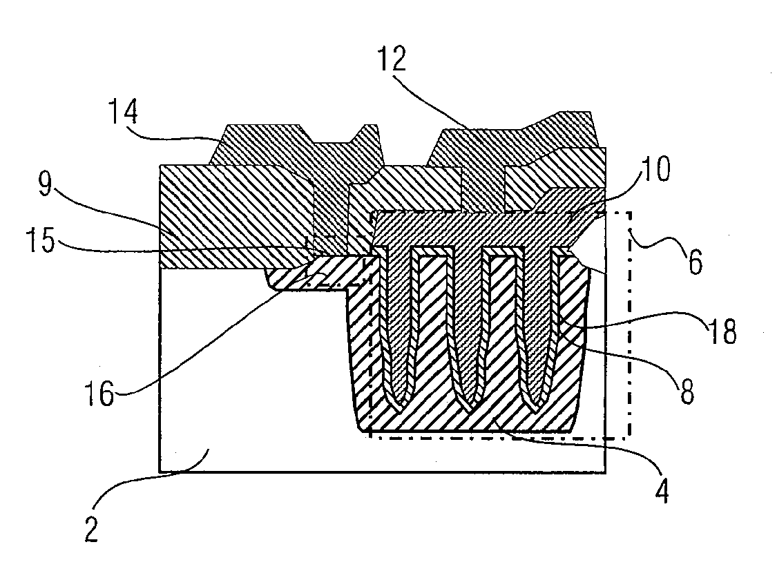
[0050]FIG. 3a shows a cross-sectional view of an inventive embodiment of the integrated snubber device which implements an attenuation network as is shown in FIG. 3b. The integrated snubber device comprises a semiconductor chip 2 having a semiconductor area 4 defined therein which represents a bottom electrode of a capacitor structure 6. Capacitor structure 6 further includes a dielectric layer 8 and a top electrode 10, the dielectric layer 8 being sandwiched between the top electrode 10 and the substrate area 4. The top electrode 10 is conductively connected to a first contact 12, and substrate area 4 is conductively connected to a second contact 14. Besides, contacts 12 and 14 are isolated from substrate 2 by an isolating layer 9. A resistor structure 16 is formed between capacitor area 6 and terminal 14 by semiconductor area 4.

[0051]In this embodiment, a contact 12 for the top electrode, and contact 14 for the bottom electrode of the capacitor structure are located on the top fac...


PUM


Abstract

Integrated snubber device on a semiconductor basis for wiring an electric network for absorbing electric energy from an electric energy store, of an electric network, including at least two terminals for being connected to the electric network to be wired, an electric resistor structure, and a reactance structure, which are connected between the terminals.

Description

CROSS-REFERENCE TO RELATED APPLICATION [0001]This application claims priority from German Patent Application No. 102006017487.9, which was filed on Apr. 13, 2006, and is incorporated herein by reference in its entirety.BACKGROUND OF THE INVENTION[0002]1. Field of the Invention[0003]The present invention-relates to the wiring, or connecting, of electric networks for switching load reduction, voltage limitation and / or oscillation attenuation, in particular to the utilization of monolithically integrated snubber devices for the above-mentioned purposes in power electronics and high-frequency engineering.[0004]2. Description of Prior Art[0005]In electronic circuits, with each switching operation there is a risk of exciting parasitic oscillations. This is intended to mean oscillations within resonant circuits formed from undesired electric energy stores, i.e. parasitic inductances and capacitances. In real devices and assembly techniques, these parasitic elements are, in principle, inevi...

Claims


Application Information

Patent Timeline
Patent Type & Authority Applications(United States)
IPC IPC(8): H02H3/20
CPCH01L23/642H01L23/647H01L27/0288H01L27/0676H01L27/0682H01L29/945H01L2924/09701H01L2924/0002H01L2924/19105H01L2924/3011H03K17/0814H01L2924/00H01L2224/48091H01L2224/48137H01L2224/48472H01L2924/12032H01L2924/13055H01L2924/13091H01L2924/00014
Inventor BERBERICH, SVENMAERZ, MARTIN
Owner FRAUNHOFER GESELLSCHAFT ZUR FOERDERUNG DER ANGEWANDTEN FORSCHUNG EV
Why Eureka
Try Eureka