Semiconductor device fabricated using a metal microstructure control process

a technology of metal microstructure and control process, which is applied in the direction of semiconductor devices, basic electric elements, electrical equipment, etc., can solve the problems of gate charge carrier depletion at the interface between the gate and the gate dielectric, the depletion of gate charge carriers, and the use of doped polysilicon gates

Active Publication Date: 2007-12-06
TEXAS INSTR INC
View PDF6 Cites 16 Cited by
  • Summary
  • Abstract
  • Description
  • Claims
  • Application Information

AI Technical Summary

Problems solved by technology

The use of doped polysilicon gates has become problematic, however, as the dimensions of gates and gate insulators alike have significantly reduced.
This limitation can result in a depletion of gate charge carriers at the interface between the gate and gate dielectric, when the gate is biased to invert the channel.
Consequently, the electrical thickness of the gate stack is substantially increased, thereby deteriorating the performance characteristics of the transistor.
In the manufacture of semiconductor devices, having independently adjustable dual work function metal gates has been troublesome, however.
However, during fabrication pro

Method used


Image

  • Semiconductor device fabricated using a metal microstructure control process
  • Semiconductor device fabricated using a metal microstructure control process
  • Semiconductor device fabricated using a metal microstructure control process

Examples


Embodiment Construction

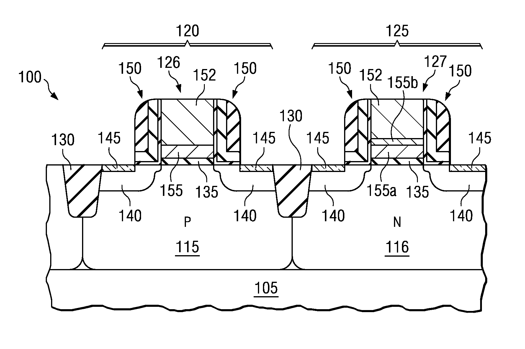
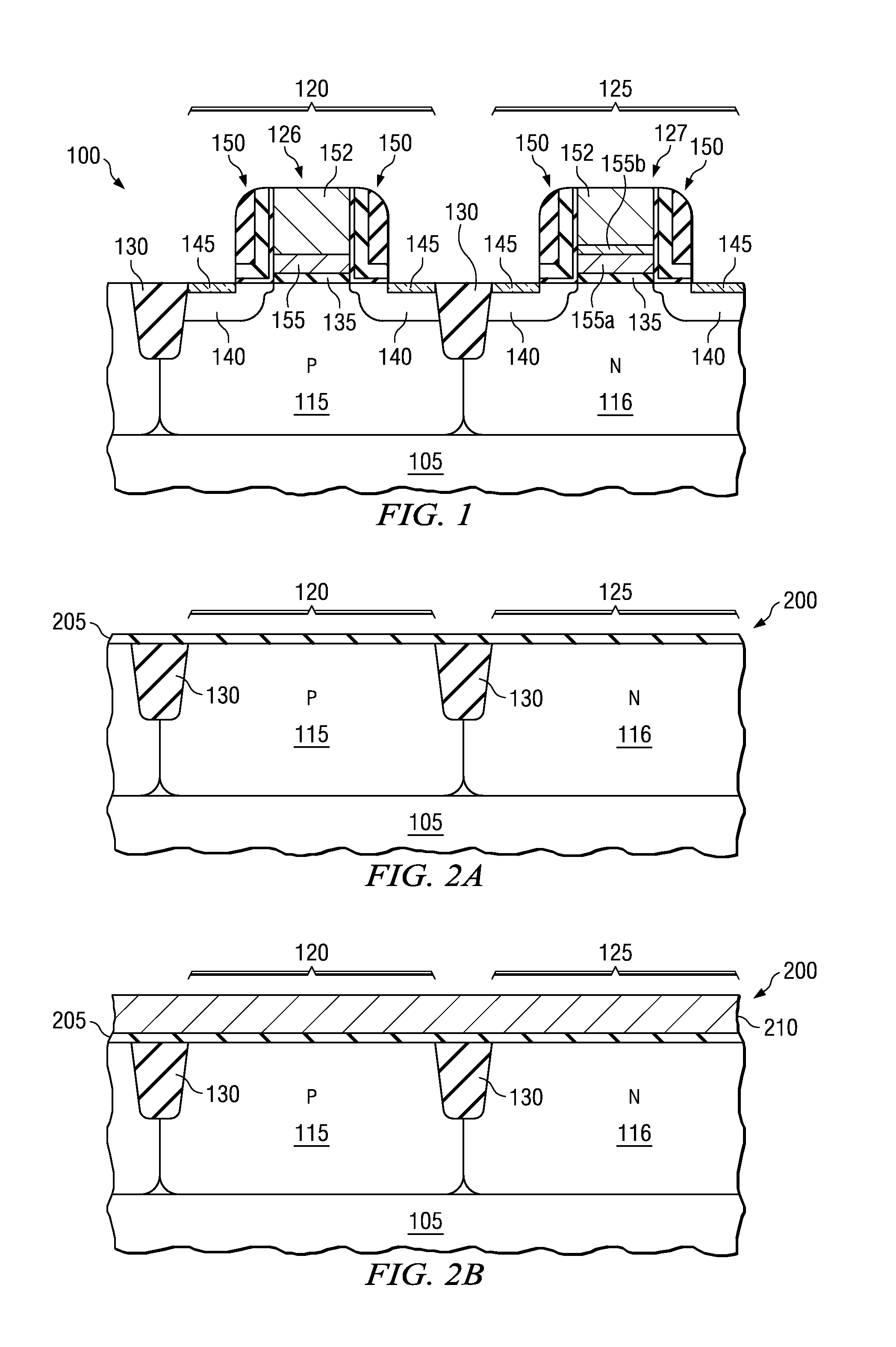
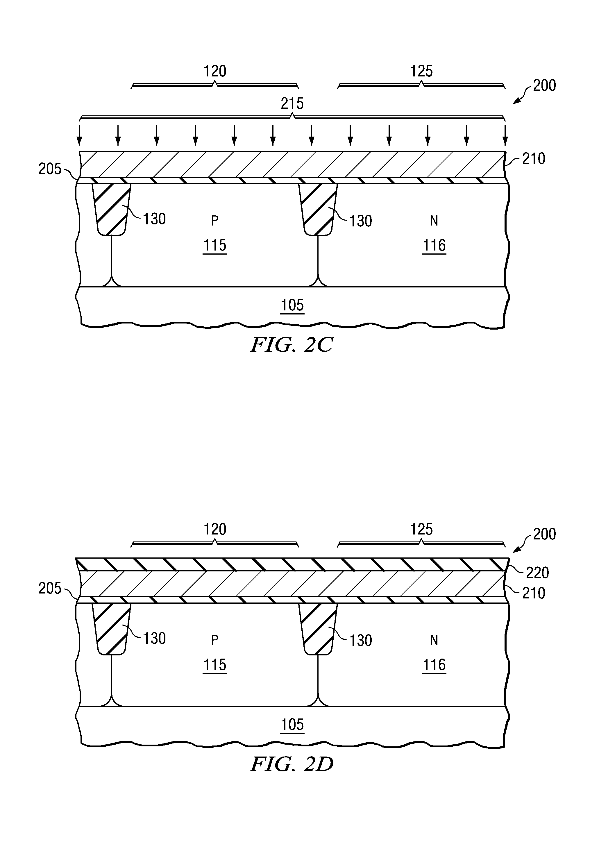
[0015]The invention overcomes previous difficulties in the production of devices having metal gates by providing a process that allows for a more uniform crystal orientation for like devices across the wafer and thereby a more uniform work function for those devices.

[0016]The term, work function, is well known and defined as the minimum energy required to bring an electron from the Fermi level to the vacuum level. A gate's work function is typically matched to one of a conduction band or a valence band of a semiconductor substrate when the work function is within about 0.4 eV, and more preferably about 0.2 eV, of the energy level of the substrate's conduction band or valence band. As an example, a gate's work function is matched to a silicon substrate's valence band when the gate work function is greater than about 4.8 eV, and more preferably between about 4.9 and about 5.2 eV. Alternatively a gate's work function is matched to a silicon substrate's conduction band when the gate wor...


PUM


Abstract

The invention provides a method for manufacturing a semiconductor device that comprises placing a metallic gate layer over a gate dielectric layer where the metallic gate layer has a crystallographic orientation, and re-orienting the crystallographic orientation of the metallic gate layer by subjecting the metallic gate layer to a hydrogen anneal.

Description

TECHNICAL FIELD OF THE INVENTION[0001]The invention is directed in general to semiconductor devices and, more specifically, to a semiconductor device fabricated using a metal microstructure control process.BACKGROUND[0002]The ability to dope polysilicon gates to different degrees allows one to adjust the work function of gate electrode materials to particular types of metal oxide silicon (MOS) transistors. It is desirable to adjust the work function of a gate electrode or gate, to be close to either the conduction band or the valence band of silicon, because this reduces the threshold voltage (Vt) of the transistor, thereby facilitating a high drive current at low operating voltages. Dual work function gates, for example doped polysilicon, are advantageously used in semiconductor devices, such as complementary metal oxide silicon (CMOS) transistor devices, having both pMOS and nMOS transistors. The use of doped polysilicon gates has become problematic, however, as the dimensions of ...

Claims


Application Information

Patent Timeline
IPC IPC(8): H01L29/94
CPCH01L21/02068H01L21/28079H01L21/823842H01L21/321H01L21/3003
Inventor COLOMBO, LUIGICHAMBERS, JAMES J.VISOKAY, MARK R.
Owner TEXAS INSTR INC
Why Eureka
Try Eureka