[0013] In one aspect, an embodiment of the present invention creates an efficient concept for providing, for accepting or for transmitting data.
[0014] An embodiment of the present invention is based on the finding that an efficient access to a memory can be achieved by providing a memory element having a variable access rate, particularly in the case of different access rates of the components accessing the memory.
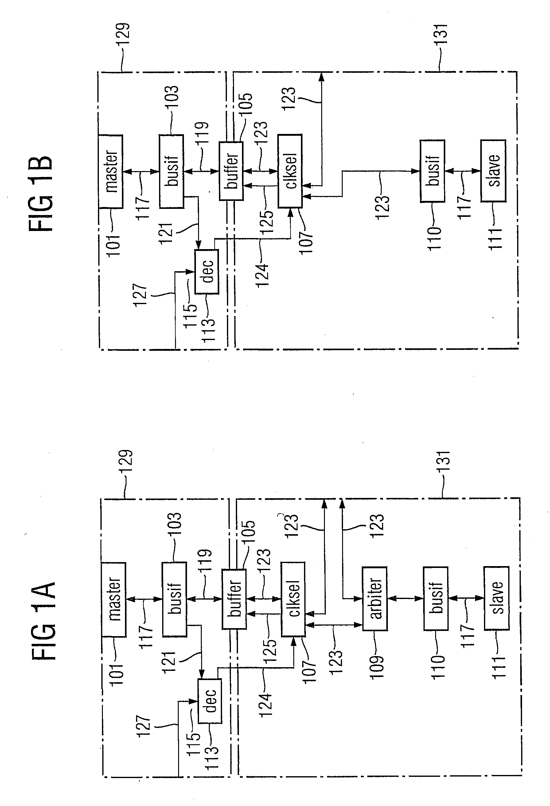
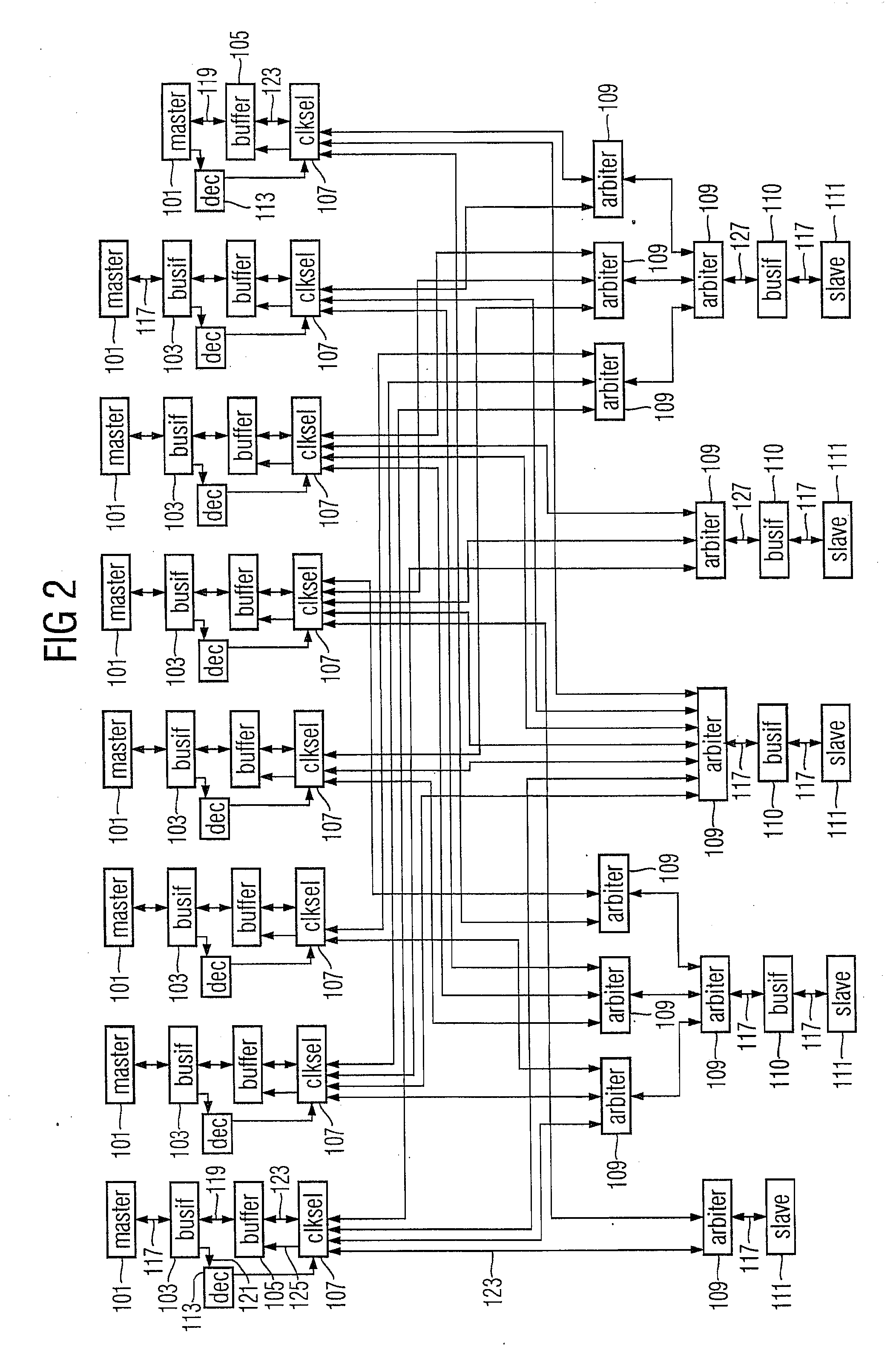
[0015] This provides, for example, an interconnect scheme in which, for example, to each master interface and to each slave interface, a separate
clock frequency can be allocated which best meets the
external interface requirements with regard to performance, wherein each master can simultaneously communicate with each slave with little latency and with a high
throughput. The interconnect scheme, for example, a crossbar, does not therefore need to be newly designed when the
clock speeds of the entities connected are changed. Since, for example, a single memory allocated to the master can serve a plurality of slaves operating at different
clock rates, the area needed for implementing the interconnect screen can be reduced, according to the invention, so that the arrangement can be implemented with all connected components on a
single chip.
[0016] According to a first embodiment, the present invention creates a memory
system with a selection element for selecting a selectable access rate from a plurality of access rates. The task of the selection element is, for example, the selection of a time base (e.g., of a
clock signal) or of two time bases for establishing the access rate and of a
data path so that data can be transmitted with the selected access rate. The second access rate is necessary when master and slave wish to transfer data at different access rates. The memory
system also comprises a memory element for providing or for accepting data at the selectable access rate which has been selected by the selection element. The access can be, for example, a memory access or a read access. According to the invention, the access rate is the rate of storing (or writing) into the memory element or of reading from the memory element or at which the memory element accepts or provides data. In this arrangement, the access rates can be different for the write operation and for the read operation. The result is that several and different communication units which are operated, for example, at different clock rates can access the same memory element without previous and complex clock conversion being necessary. This makes it possible that, for example, a master with a single memory element can operate a plurality of slaves operated at different clock rates, which, for example, access the memory element at different access rates. This reduces the number of memories because there is no need for providing a memory for each slave.
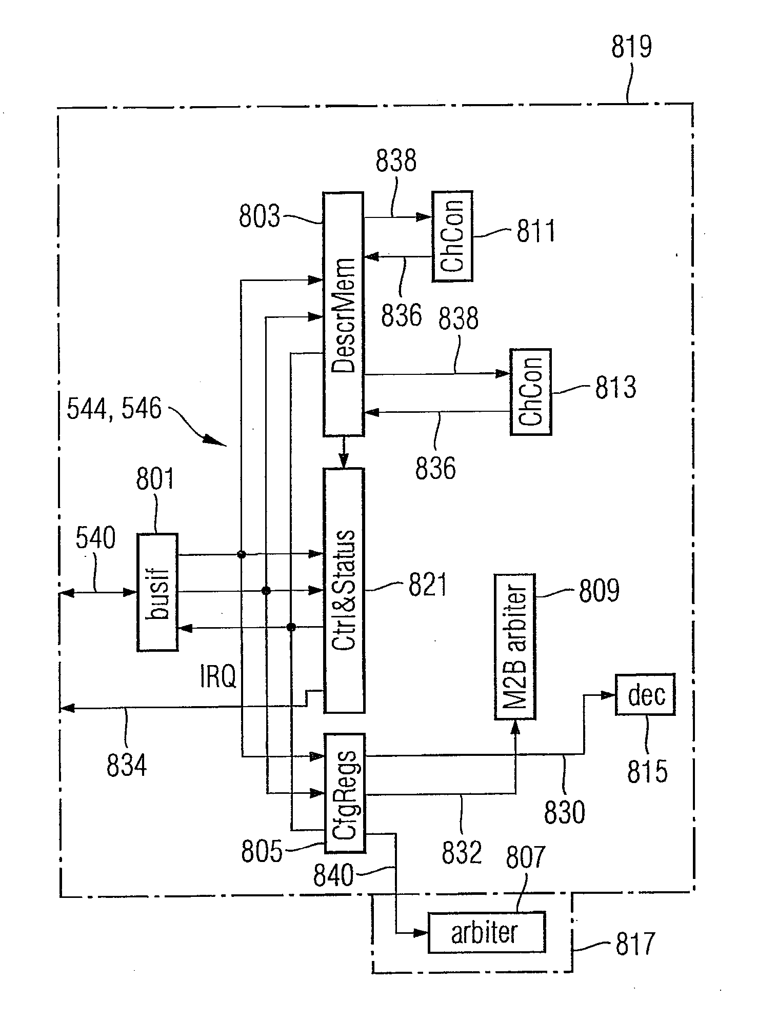
[0050] The access to the respective
memory interface is controlled by using the
access control elements. The first and the second
access control element preferably have the same functionality. According to a further embodiment, the first and the second
access control element are of identical structure. This has the result that it is already possible during the design of a memory communication system with an arbitrary number of interfaces, to access access control elements already designed which, for example, can be allocated virtually by means of “copy and paste” to the interfaces to be added, which reduces design costs. If the memory communication system according to an embodiment of the invention is arranged, for example, as a DMA system, a standard design can be established which is independent of the number of interfaces and of the number of memories connected to the interfaces due to the modular allocation of identical access control elements which can be arranged, for example, as channel controllers or memory controllers.

