Integrated Circuit Packaging

a technology of integrated circuits and packaging, which is applied in the direction of printed circuit manufacturing, electrical apparatus casings/cabinets/drawers, coupling device connections, etc., can solve the problems of poor heat transfer characteristics, affecting the tilt of the lid, and non-uniform thickness of thermal interface materials

Active Publication Date: 2007-12-13
ADVANCED MICRO DEVICES INC
View PDF35 Cites 16 Cited by
  • Summary
  • Abstract
  • Description
  • Claims
  • Application Information

AI Technical Summary

Problems solved by technology

High tilt can lead to nonuniformities in thermal interface material thickness, which can produce poor heat transfer characteristics.
Indium as a thermal interface material presents certain challenges.
Furthermore, the aforementioned tilt of the lid may be impacted by thermally-induced movement of the lid adhesive during steps to bond the indium.
Trapped flux remnants can result in the formation of voids in the indium.
Depending on the location of these “hot spots,” device performance can be adversely impacted.
An issue associated with conventional gold films is the possibility that there will insufficient indium near the corners of the die after reflow.
With insufficient indium at the corners, stresses applied to the indium can cause significant cracking of the indium preform after the repeated thermal cycling that occurs during normal device operation.
The cracks create areas of heightened thermal resistance and thus hot spots.
A glob, if large enough and in the right spot, may touch and damage or short external devices, such as capacitors.

Method used


Image

  • Integrated Circuit Packaging
  • Integrated Circuit Packaging
  • Integrated Circuit Packaging

Examples


Embodiment Construction

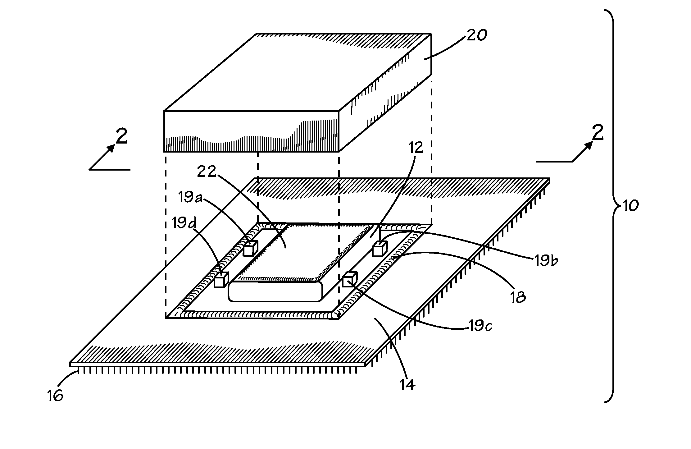
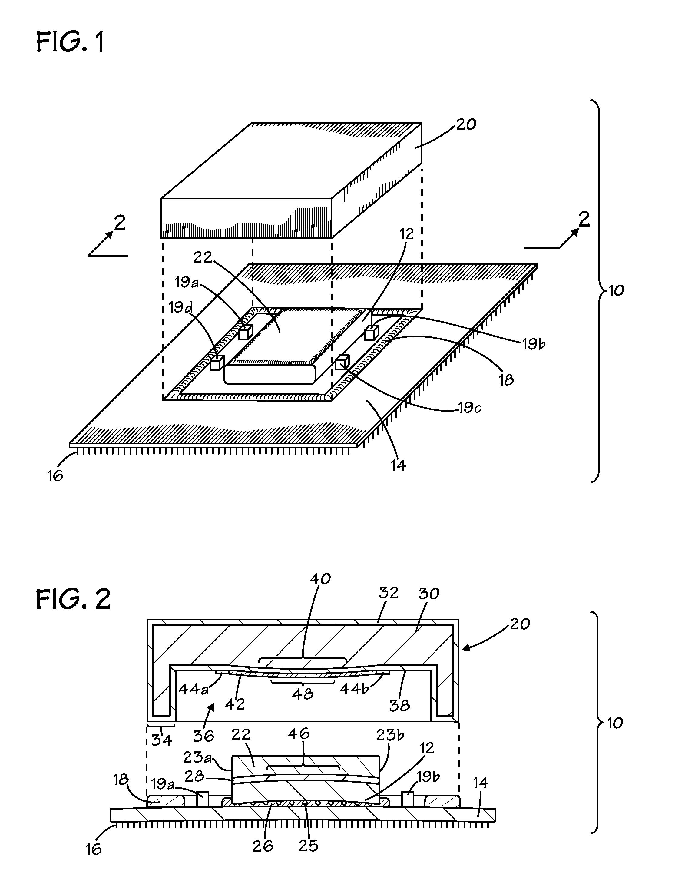
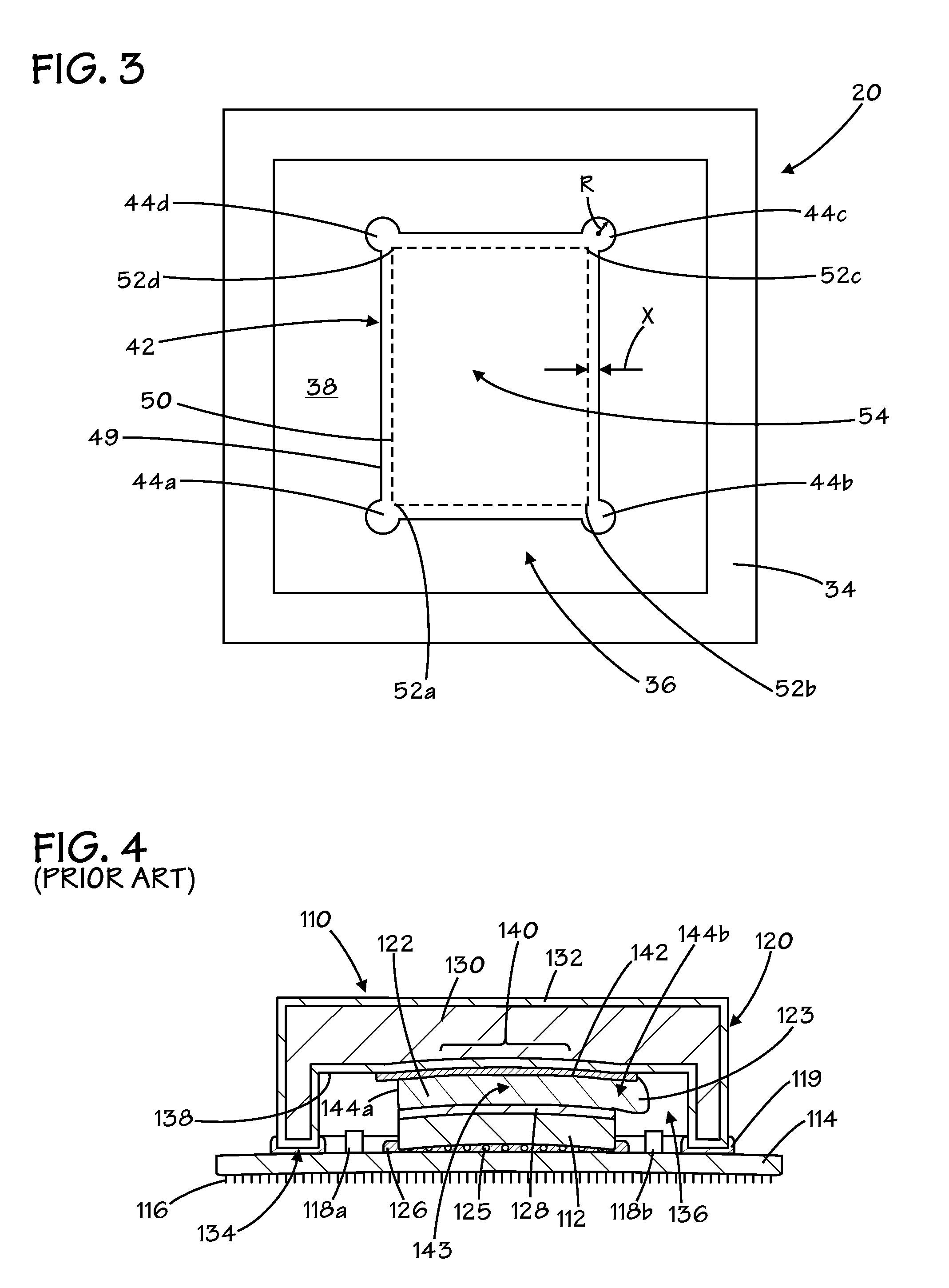
[0035]In the drawings described below, reference numerals are generally repeated where identical elements appear in more than one figure. Attention is now turned to FIGS. 1 and 2. FIG. 1 is an exploded pictorial view and FIG. 2 is a sectional view of an exemplary embodiment of an integrated circuit package 10 that includes an integrated circuit 12 mounted on a substrate 14. The substrate 14 may be provided with a plurality of conductor pins 16 that form a pin grid array or other pin-type arrangement for providing electrical connection to a socket or other type of electrical connection. Optionally, the substrate 14 may utilize some other form of interconnect, such as, for example, a land grid array or other types of interconnect structures. The integrated circuit 12 is electrically connected to one or more external electronic devices, four of which are visible and labeled 18a, 18b, 18c and 18d. The external devices 18a, 18b, 18c and 18d are typically capacitors, but may also be resis...


PUM

PropertyMeasurementUnit
sizeaaaaaaaaaa
temperatureaaaaaaaaaa
pressureaaaaaaaaaa

Abstract

Various integrated circuit package elements are provided. In one aspect, an integrated circuit package device is provided that includes a lid for covering an integrated circuit. The lid has a convex surface for applying pressure on the integrated circuit when the lid is placed in a selected position. In another aspect, an integrated circuit package device is provided that includes a lid that has a surface for applying pressure to an integrated circuit when the lid is in a selected position. A gold film is coupled to the surface. The gold film has a periphery and a plurality of rounds extending from the periphery.

Description

BACKGROUND OF THE INVENTION[0001]1. Field of the Invention[0002]This invention relates generally to semiconductor processing, and more particularly to methods of and apparatus for packaging an integrated circuit.[0003]2. Description of the Related Art[0004]Many current integrated circuits are formed as multiple die on a common wafer. After the basic process steps to form the circuits on the die are complete, the individual die are cut from the wafer. The cut die are then usually mounted to structures, such as circuit boards, or packaged in some form of enclosure.[0005]One frequently-used package consists of a substrate upon which a die is mounted. The upper surface of the substrate includes electrical interconnects. The die is manufactured with a plurality of bond pads. A collection of solder bumps are provided between the bond pads of the die and substrate interconnects to establish ohmic contact. After the die is mounted to the substrate, a lid is attached to the substrate to cove...

Claims


Application Information

Patent Timeline
Patent Type & Authority Applications(United States)
IPC IPC(8): H01R13/46
CPCH01L23/10H01L23/3675H01L2224/16H01L2224/73253H01L2924/01078H01L2924/01079Y10T29/49131H01L2924/16152Y10T29/4913Y10T29/49117Y10T29/49144
Inventor TOO, SEAH SUNKHAN, MOHAMMADHAYWARD, JAMESDIEP, JACQUANA
Owner ADVANCED MICRO DEVICES INC
Why Eureka
Try Eureka