Preparation method of silicon micro/nanometer line array with controllable dimension

A technology of nanowire array and silicon micro, which is applied in the field of preparation of micro/nanowire array, can solve problems such as difficult device use, and achieve the effects of low cost, simple process and low energy consumption

Inactive Publication Date: 2012-07-11
HEFEI UNIV OF TECH
View PDF4 Cites 17 Cited by
  • Summary
  • Abstract
  • Description
  • Claims
  • Application Information

AI Technical Summary

Problems solved by technology

There are many methods for synthesizing silicon micro / nanowires, such as VLS growth method, oxygen assisted growth method (OAG) and SLS growth method, but these synthesized silicon micro / nanowires have a typical random directionality, (the problem of size) is difficult to device used in

Method used


Image

  • Preparation method of silicon micro/nanometer line array with controllable dimension
  • Preparation method of silicon micro/nanometer line array with controllable dimension
  • Preparation method of silicon micro/nanometer line array with controllable dimension

Examples


Embodiment 1

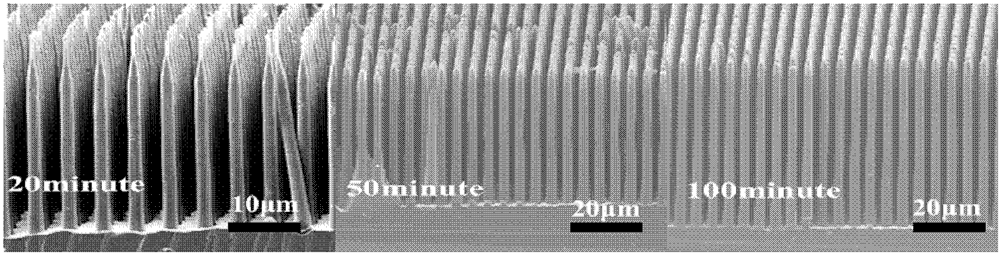
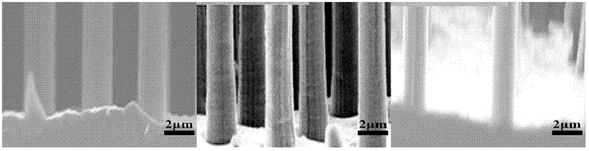
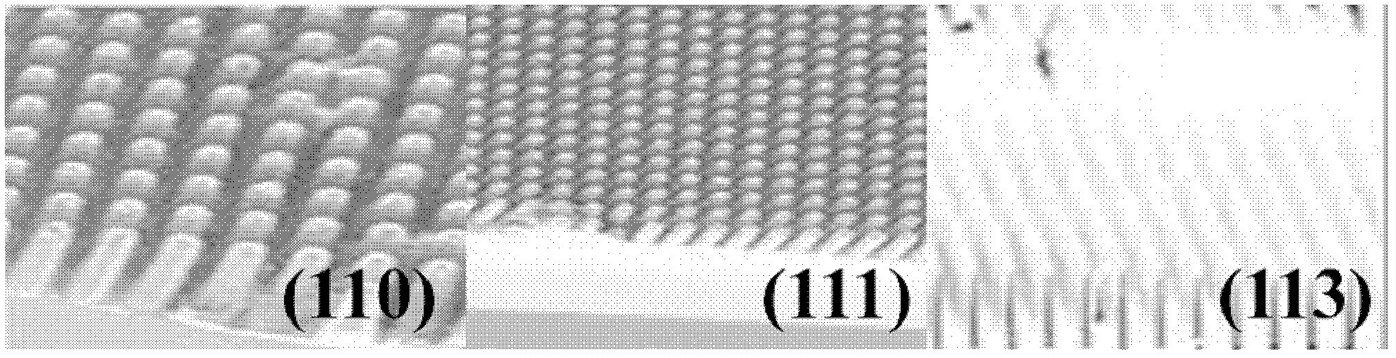
[0032] Based on the n-type silicon wafer with (100) crystal orientation and resistivity of 5Ωcm, place the silicon wafer in deionized water and acetone in sequence for ultrasonic cleaning for 15 minutes, and then immerse in piranha washing solution at 60°C After 10 minutes, take it out and dry it to be sample A. Spin-coat photoresist AZ5206 on the surface of sample A, and form a photoresist layer with a thickness of 300-500 nanometers after drying; it is made in the form of a silicon micro / nano wire array Contact mask, using a contact mask with silicon micro / nano wire array patterns to expose the photoresist layer to UV for 40s to obtain sample B, remove sample B and develop in developer MIF-300 for 4 minutes to wash away The exposed photoresist obtained sample C;

[0033] Use the method of electron beam thermal evaporation or magnetron sputtering to directly plate a gold film with a thickness of 20 nanometers on the surface of sample C to obtain sample D; place sample D in ac...

Embodiment 2

[0037] Based on the n-type silicon wafer with (100) crystal orientation and resistivity of 5Ωcm, place the silicon wafer in deionized water and acetone in sequence for ultrasonic cleaning for 15 minutes, and then immerse in piranha washing solution at 60°C After 10 minutes, take it out and dry it to be sample A. Spin-coat photoresist AZ5206 on the surface of sample A, and form a photoresist layer with a thickness of 300-500 nanometers after drying; it is made in the form of a silicon micro / nano wire array Contact mask, using a contact mask with silicon micro / nano wire array patterns to expose the photoresist layer to UV for 40s to obtain sample B, remove sample B and develop in developer MIF-300 for 4 minutes to wash away The exposed photoresist obtained sample C;

[0038] Use the method of electron beam thermal evaporation or magnetron sputtering to directly plate a gold film with a thickness of 20 nanometers on the surface of sample C to obtain sample D; place sample D in ac...

Embodiment 3

[0043]Based on n-type silicon wafer with crystal orientation of (100) and resistivity of 12 Ωcm, the silicon wafer was placed in deionized water and acetone for 15 minutes of ultrasonic cleaning, and then immersed in piranha washing solution at 60 °C After 10 minutes, take it out and dry it to be sample A. Spin-coat photoresist AZ5206 on the surface of sample A, and form a photoresist layer with a thickness of 300-500 nanometers after drying; it is made in the form of a silicon micro / nano wire array Contact mask, using a contact mask with a silicon micro / nano wire array pattern to expose the photoresist layer to UV exposure to obtain sample B, remove sample B and develop in a developer for 4 minutes to wash away the exposed photoresist Adhesive sample C;

[0044] A gold film with a thickness of 20 nanometers is directly plated on the surface of the sample C by means of electron beam thermal evaporation or magnetron sputtering to obtain a sample D; the sample D is placed in ace...


PUM

PropertyMeasurementUnit
thicknessaaaaaaaaaa
thicknessaaaaaaaaaa
thicknessaaaaaaaaaa

Abstract

The invention discloses a preparation method of a silicon micro/nanometer line array with a controllable dimension. The preparation method is characterized in that a silicon chip is used as a substrate, a sample A is obtained through taking out the silicon chip to be dried after the surface of the silicon chip is cleaned, photoresist is coated on the surface of the sample A in a spiral way, and a photoresist layer is baked; a contact type mask is prepared according to the pattern types of the silicon micro/nanometer line array, the mask is utilized for realizing the exposure on the photoresist layer to obtain a sample B, the sample B is developed in developing liquid for 4 to 6 minutes, and exposed photoresist is washed away to obtain a sample C; a gold film with the thickness being 20 to 50 nanometers is coated on the surface of the sample C to obtain a sample D; the sample D is placed into acetone to remove the photoresist and the gold on the sample, and the silicon chip in contact with the gold, i.e. a sample E is obtained; and the sample E is soaked into etching liquid to carry out gold catalysis chemical etching, and the silicon micro/nanometer line array is obtained after the etching completion. The preparation method provided by the invention can be used for obtaining the silicon micro/nanometer line array with the controllable diameter and length and the uniform crystal orientation so that the silicon micro/nanometer line array can realize the practical application to devices.

Description

technical field [0001] The invention relates to a method for preparing silicon micro / nano wire arrays, more specifically a method for preparing silicon micro / nano wire arrays by chemically etching silicon through metal catalysis. Background technique [0002] In recent years, the semiconducting, mechanical, and optical properties of one-dimensional silicon micro / nanowires, as well as the promising applications of nanodevices have attracted widespread attention. Silicon micro / nanowires have been successfully used in field effect transistors, biochemical sensors, integrated logic devices, solar cells, lithium battery anodes, p-n junctions and other devices. There are many methods for synthesizing silicon micro / nanowires, such as VLS growth method, oxygen assisted growth method (OAG) and SLS growth method, but these synthesized silicon micro / nanowires have typical random orientation, which is difficult to produce in the used in the device. Contents of the invention [0003]...

Claims


Application Information

Patent Timeline
Patent Type & Authority Applications(China)
IPC IPC(8): B81C1/00
Inventor 罗林保揭建胜聂彪吴春艳于永强
Owner HEFEI UNIV OF TECH
Why Eureka
Try Eureka