Preparation method for orderly silicon nanowire array

A silicon nanowire and orderly technology, applied in the field of nanomaterial preparation and application, can solve the problems of high cost and low efficiency, and achieve the effect of low cost, low cost and simple method

Inactive Publication Date: 2013-05-22
ANHUI NORMAL UNIV
View PDF1 Cites 16 Cited by
  • Summary
  • Abstract
  • Description
  • Claims
  • Application Information

AI Technical Summary

Problems solved by technology

Reactive ion etching needs to be combined with photolit

Method used


Image

  • Preparation method for orderly silicon nanowire array
  • Preparation method for orderly silicon nanowire array

Examples


Embodiment Construction

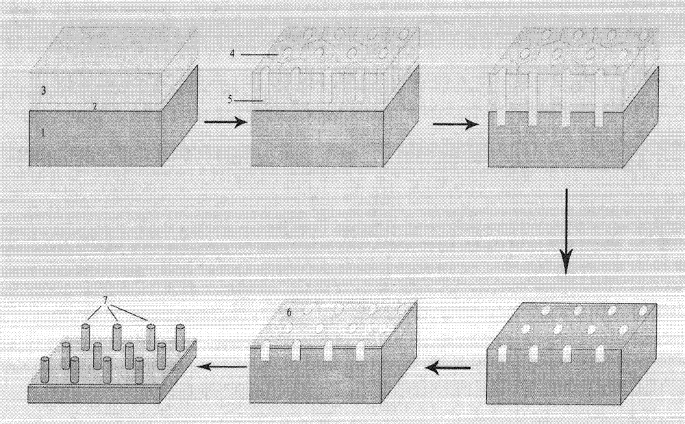
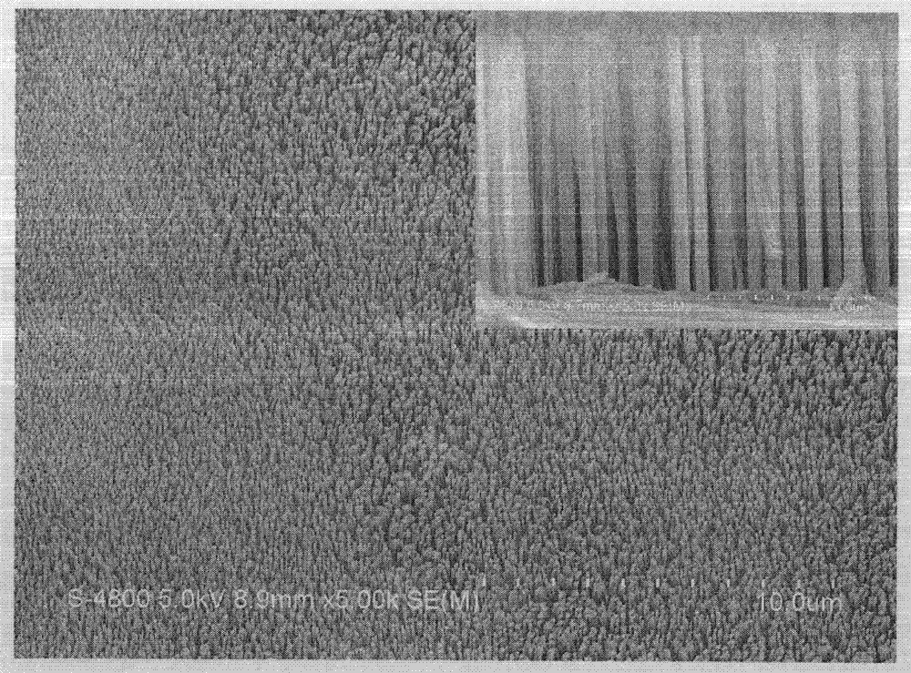
[0022] Refer to the attached figure 1 The specific steps of the method of the present invention are described in detail.

[0023] (1) Select a suitable silicon substrate 1 and perform ultrasonic treatment on the silicon wafer with acetone and ethanol respectively to remove surface contamination and organic matter. Further, concentrated sulfuric acid and hydrogen peroxide solution are used to clean the silicon wafer, and after rinsing with deionized water, dilute hydrofluoric acid solution is used to remove surface oxides, and then rinsed repeatedly with deionized water.

[0024] (2) Deposit a layer of silicon oxide 2 with a thickness of 20-80 nm on the cleaned silicon surface by using plasma chemical vapor deposition equipment.

[0025] (3) Deposit aluminum film 3 with a thickness of 200-500nm on the surface of silicon oxide by thermal evaporation or electron beam evaporation, and the background vacuum of the cavity is 2-8×10 -4 Pa, the initial deposition rate is about 0.1n...


PUM


Abstract

The invention relates to a preparation method for an orderly silicon nanowire array. A porous alumina template and metal auxiliary chemical corrosion are combined to obtain the orderly silicon nanowire array. The preparation method for the orderly silicon nanowire array comprises the following steps: sequentially depositing a SiO2 film and an aluminum (Al) film on a clean silicon chip surface; then anodizing the aluminum (Al) film to form porous aluminum oxide (AAO); etching on the silicon surface by means of plasma with the AAO as the masking to copy a hole array graph of the AAO; removing AAO layer and SiO2 layer, depositing a gold film on a graphical silicon surface, and obtaining a gold layer of a mesh structure; enabling a sample of the gold film which is covered with the mesh structure to be immersed into hydrofluoric (HF) acid and H2O2 corrosive liquid to corrode, and finally obtaining a silicon nanowire array. The preparation method for the orderly silicon nanowire array is easy, and a large-area orderly and vertically arranged silicon nanowire array can be prepared; the facts that trends, doping types and levels, diameters, lengths, separation distances, surface densities and the like of the nanowire array are effectively controlled can be achieved, and cost is low, and therefore the preparation method for the orderly silicon nanowire array can be used for a device based on a silicon nanowire array.

Description

technical field [0001] The invention relates to a preparation method of silicon nanowires, in particular to a preparation method of a vertical silicon nanowire array with large-area arrangement, uniform and controllable diameter and length, and belongs to the technical field of nanomaterial preparation and application. Background technique [0002] Silicon nanowires have attracted widespread attention due to their excellent properties and good process compatibility, and have great stress prospects in advanced electronic devices, biological and chemical sensors, optoelectronic devices, and photovoltaic devices. The controllable preparation of silicon nanowires is a prerequisite for its application. Various top-down and bottom-up techniques, such as solid-liquid-gas (VLS) growth, electrochemical etching, reactive ion etching, and metal-assisted chemical etching, all have significant influence on the relevant parameters of nanowires. A certain amount of control. Among them, V...

Claims


Application Information

Patent Timeline
IPC IPC(8): B82B3/00B82Y40/00
Inventor 左则文
Owner ANHUI NORMAL UNIV
Why Eureka
Try Eureka