Optoelectronic device and method of making same

Active Publication Date: 2007-12-20
VI SYST GMBH
View PDF2 Cites 31 Cited by
  • Summary
  • Abstract
  • Description
  • Claims
  • Application Information

AI Technical Summary

Benefits of technology

[0031]One another embodiment includes an apparatus, wherein a light-emitting device comprises, instead of a multilayer interference reflector, an evanescent reflector. And ...

Problems solved by technology

The interference can be constructive or destructive,...

Method used


Image

  • Optoelectronic device and method of making same
  • Optoelectronic device and method of making same
  • Optoelectronic device and method of making same

Examples


first embodiment

[0107]FIG. 11(a) shows an apparatus (1000), according to the present invention, the apparatus comprising a light-emitting device (1010), an external cavity (1030), and one or a plurality of external mirrors. Since the light-emitting device emits light at some angle with respect to the direction (1005) normal to the surface plane, the far-field diagram is typically multi-lobe. Correspondingly, more than one external mirror is used. A preferred embodiment includes a light-emitting device emitting light in two lobes, an external cavity, and two external mirrors, a first mirror (1014) and a second mirror (1024). In this embodiment distance between the exit surface of the light-emitting device (1010) and the mirrors is large, and the major part of the cavity (1030) is a far-field zone of the light-emitting device (1010), where propagation of light obeys the laws of the geometrical optics. Light emitted at angles such that it does not impinge on the mirrors, is lost. Only light emitted a...

second embodiment

[0109]FIG. 11(b) shows the present invention, where the apparatus (1050) contains a second mirror (1074) as a flat mirror, and a collecting lens (1056) is used to focus light onto the mirror or onto the surface of the surface-emitting device. Wavelength-stabilized laser light (1065) comes out through a semi-transparent collecting mirror (1014). In another embodiment of the present invention, a semi-transparent mirror is flat, and a collecting lens is located between this mirror and the surface-emitting device. In one another embodiment, both mirrors are flat, and collecting lenses are placed on both sides of the surface-emitting device.

[0110]It is important to emphasize a dramatic difference between the wavelength-selective tilted cavity laser of the prior art and the wavelength selective laser of the present invention. In a tilted cavity laser, the wavelength selection is governed by the intersection of the dispersion law of a cavity and of that of a MIR. The dispersion law of the ...

third embodiment

[0112]FIG. 11(c) shows an apparatus for frequency conversion (1100) according to the present invention. A non-linear crystal is located within the cavity. The apparatus comprising a light-emitting device (1010), an external cavity (1030), a first mirror (1114), and a second non-transparent mirror (1074) generates wavelength-stabilized primary laser light. The optical path of the laser light at the first harmonic goes through a non-linear crystal (1110), where a second harmonic of light is generated. All mirrors are preferably non-transparent for the primary light. One mirror (1114) is preferably semi-transparent for the generated second harmonic of light. Laser light at second harmonic (1115) comes out through the mirror (1114).

[0113]It should be noted that the optical path of light is tilted with respect to the surface of the light-emitting device. An advantage of this approach, among others, is that the optical power in the nonlinear crystal is enhanced by the factor 1 / cos , and t...


PUM


Abstract

A light emitting device is disclosed that emits light from the surface in a broad spectral range and in a broad range of angles tilted with respect to the direction normal to the exit surface. An apparatus for generating wavelength-stabilized light is formed of a light-emitting device, an external cavity and at least one external mirror. Light emitted by the light-emitting device at a certain preselected angle, propagates through the external cavity, impinges on the external mirror and is reflected back. Light emitted at other angles does not impinge on the external mirror. Thus, a feedback occurs only for the light emitted at a preselected angle. Light impinged on the external mirror and reflected back undergoes interference with the emitted light. The interference can be constructive or destructive. Constructive interference results in a positive feedback. The positive feedback occurs, if light emitted by the light-emitting device is reflected back and reaches the active region in phase, i.e. if the phase matching between emitted and reflected light waves occurs. The positive feedback conditions are met at one or a few selected wavelengths within the luminescence spectrum of the active region. Then the apparatus generates wavelength-stabilized light. In different embodiments, an apparatus may operate as a wavelength-stabilized light-emitting diode, a wavelength-stabilized superluminescent light-emitting diode, or a wavelength-stabilized laser.
Various embodiments are possible which are distinguished in a way of optical coupling between a light-emitting device and an external mirror. The coupling can be realized via the far-field zone of the light emitted by the light-emitting device, via the near-field zone, or via a single epitaxial structure.
An apparatus for the frequency conversion is disclosed further comprising a non-linear crystal located within the external cavity.

Description

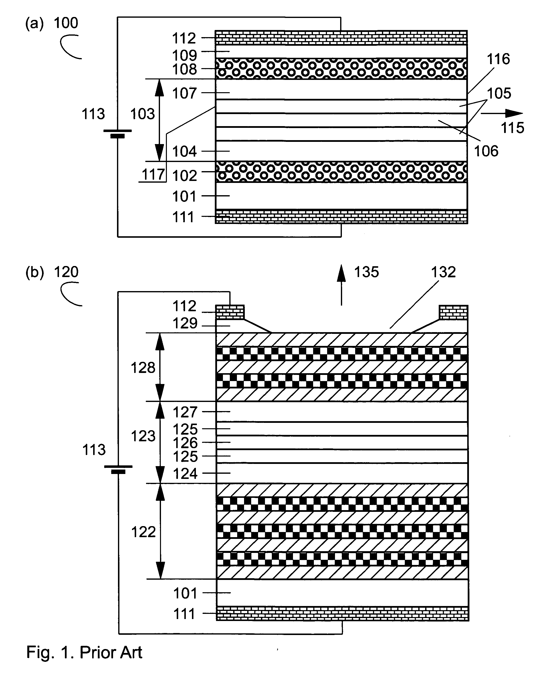
REFERENCE TO RELATED APPLICATIONS[0001]This application claims an invention which was disclosed in Provisional Application No. 60 / 814,053, filed Jun. 16, 2006, entitled “SURFACE-EMITTING OPTOELECTRONIC DEVICE AND METHOD OF MAKING SAME”. The benefit under 35 USC § 19(e) of the United States provisional application is hereby claimed, and the aforementioned application is hereby incorporated herein by reference.BACKGROUND OF THE INVENTION[0002]1. Field of the Invention[0003]The invention pertains to the field of semiconductor devices. More particularly, the invention pertains to light-emitting diodes, wavelength-stabilized semiconductor edge-emitting and surface-emitting lasers, optical amplifiers, photodetectors, and mode-locked lasers.[0004]2. Description of Related Art[0005]A prior art semiconductor diode laser, or more specifically, edge-emitting laser, is shown in FIG. 1(a). The laser structure (100) is grown epitaxially on an n-doped substrate (101). The structure further include...

Claims


Application Information

Patent Timeline
IPC IPC(8): H01S3/00
CPCG02F2001/3542H01L33/105H01S5/005H01S5/0092H01S5/0421H01S5/0425H01S5/2027H01S5/1032H01S5/1035H01S5/1096H01S5/14H01S5/183H01S5/18305H01S5/1021G02F1/3542H01S5/18361
Inventor LEDENTSOV, NIKOLAISHCHUKIN, VITALY
Owner VI SYST GMBH
Why Eureka
Try Eureka