Substrate Processing Method and Substrate Processing Apparatus

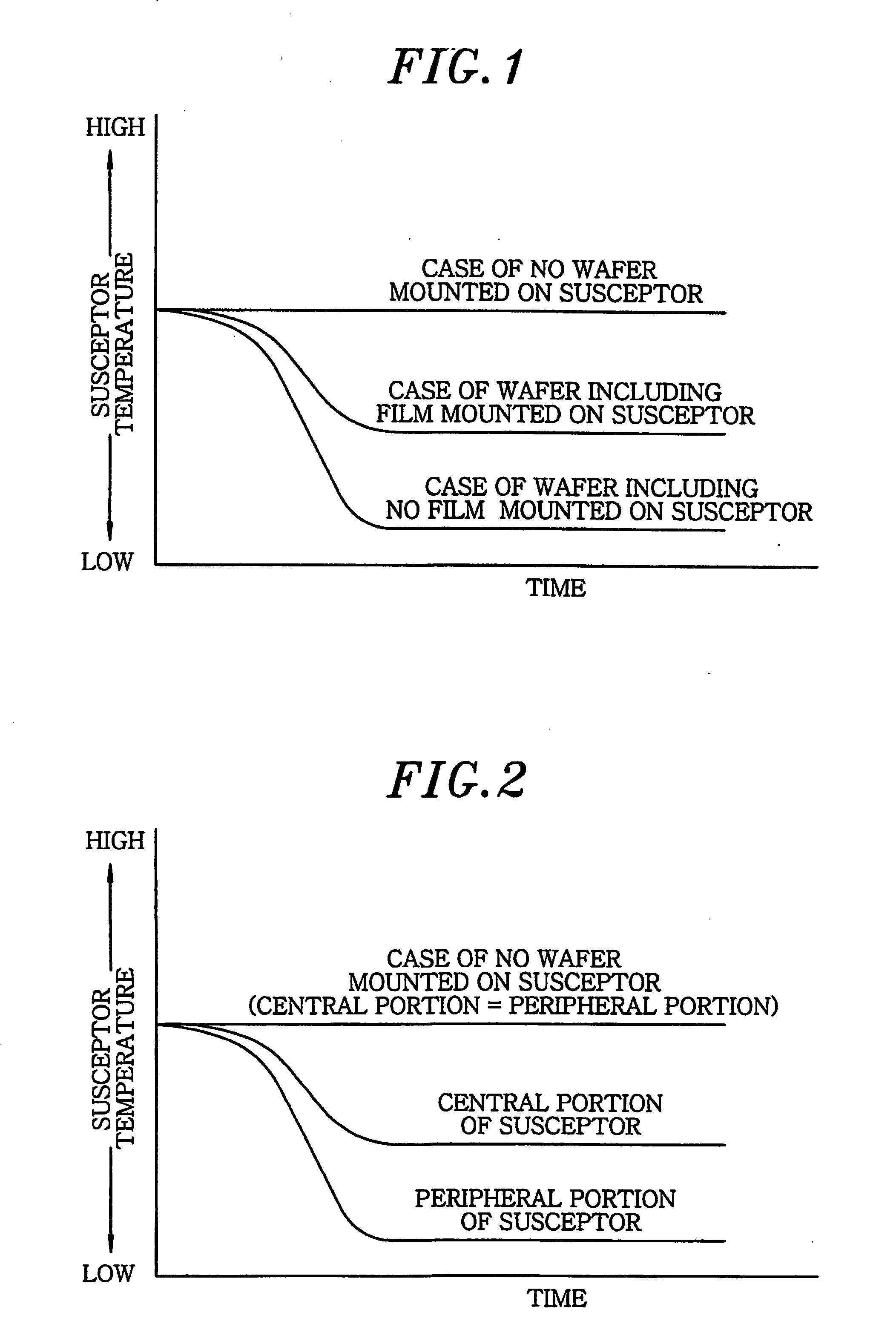
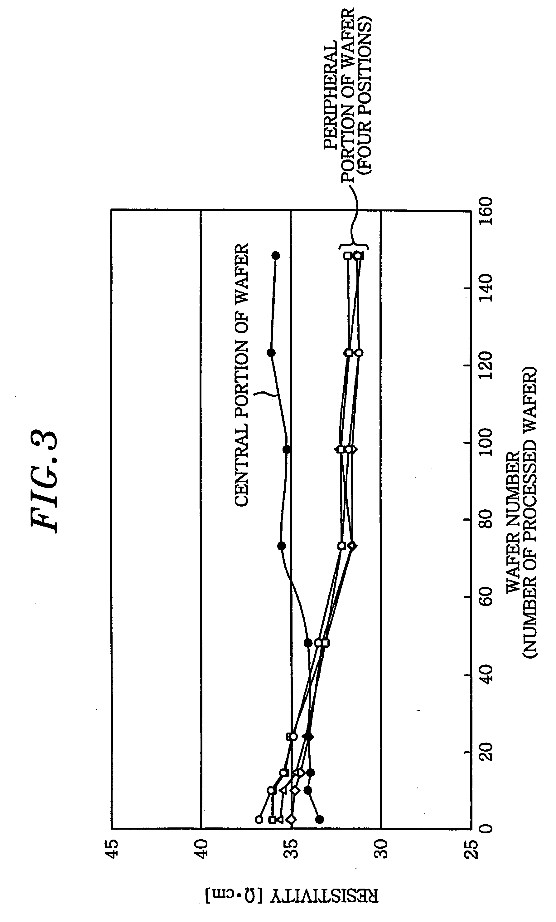
a substrate processing and substrate technology, applied in the direction of semiconductor/solid-state device testing/measurement, chemical vapor deposition coating, coating, etc., can solve the problem of difficult to select the optimal temperature condition for every wafer, the thermal absorption of the wafer can get different, and the quality or reliability of the final semiconductor device is deteriorated. , to achieve the effect of improving the in-surface uniformity of processing, preventing the variation of temperature in the surface of the substrate, and improving the reprodu

Inactive Publication Date: 2007-12-20
TOKYO ELECTRON LTD
View PDF6 Cites 27 Cited by
  • Summary
  • Abstract
  • Description
  • Claims
  • Application Information

AI Technical Summary

Benefits of technology

[0011] It is, therefore, an object of the present invention to provide a substrate processing method and a substrate processing apparatus capable of performing a high-precision processing by increasing precision of temperature control to improve a processing reproducibility between different types of wafers and also improve in-surface uniformity of processing for a wafer.
[0032] In accordance with the present invention, by measuring a thermal characteristic of the substrate to be processed in advance and controlling temperatures at plural regions of the substrate independently based on a measured value of the thermal characteristic, it is possible to improve a processing reproducibility between different types of wafers and also improve in-surface uniformity of processing for a wafer.
[0033] In other words, by measuring the thermal characteristic of a substrate to be processed, it is possible to perform a control corresponding to an inherent behavior of temperature variation of the substrate depending on the type of the substrate. Furthermore, the heating temperatures for the plural regions of the substrate are independently controlled by, e.g., the respective heaters, so that it is possible to prevent the variation of temperature in the surface of the substrate.
[0034] Accordingly, the temperature of the substrate can be controlled with a high precision to prevent, e.g., variation in resistivity (Rs) and nonuniformity of film thickness in the surface thereof, so that the quality of a semiconductor device and the like can be enhanced.

Problems solved by technology

Any problem in the temperature control can directly lead to deterioration of the quality or reliability of final semiconductor devices.
However, if types of wafers (i.e., types of films formed on the wafers, types and concentrations of doped impurities therein, etc.) are different, thermal absorptances of the wafers can get different, so that it has been difficult to select an optimal temperature condition for every wafer when processing different types of wafers successively.
Further, even in case the types of the wafers are identical, there may occur a difference in behaviors of the temperatures of, e.g., a central region and a peripheral region of the susceptor corresponding to the central portion and the peripheral portion of the wafers, respectively, which would result in deterioration in quality of the wafers after the film formation.
In these methods, though it is possible to improve inter-wafer reproducibility of processing, the technique to perform different controls depending on the areas of the wafers is not considered at all.
Thus, the methods are insufficient to improve in-surface uniformity in a wafer (e.g., in-surface uniformity in quality and thickness of films formed on the wafer).
However, in case the temperature detecting unit cannot be installed at other locations than the central region of the susceptor due to a restriction from, e.g., a heater structure, it is impossible to correctly detect temperatures at the susceptor's other regions (for example, a peripheral region of the susceptor) where no temperature detecting unit is installed while the temperature of the central portion can be measured.
With the conventional methods, however, it is difficult to correct heating conditions while improving the in-surface uniformity of the processing temperature for the wafer.

Method used


Image

  • Substrate Processing Method and Substrate Processing Apparatus
  • Substrate Processing Method and Substrate Processing Apparatus
  • Substrate Processing Method and Substrate Processing Apparatus

Examples


Embodiment Construction

[0047] Hereinafter, exemplary embodiments of the present invention will be described with reference to the accompanying drawings.

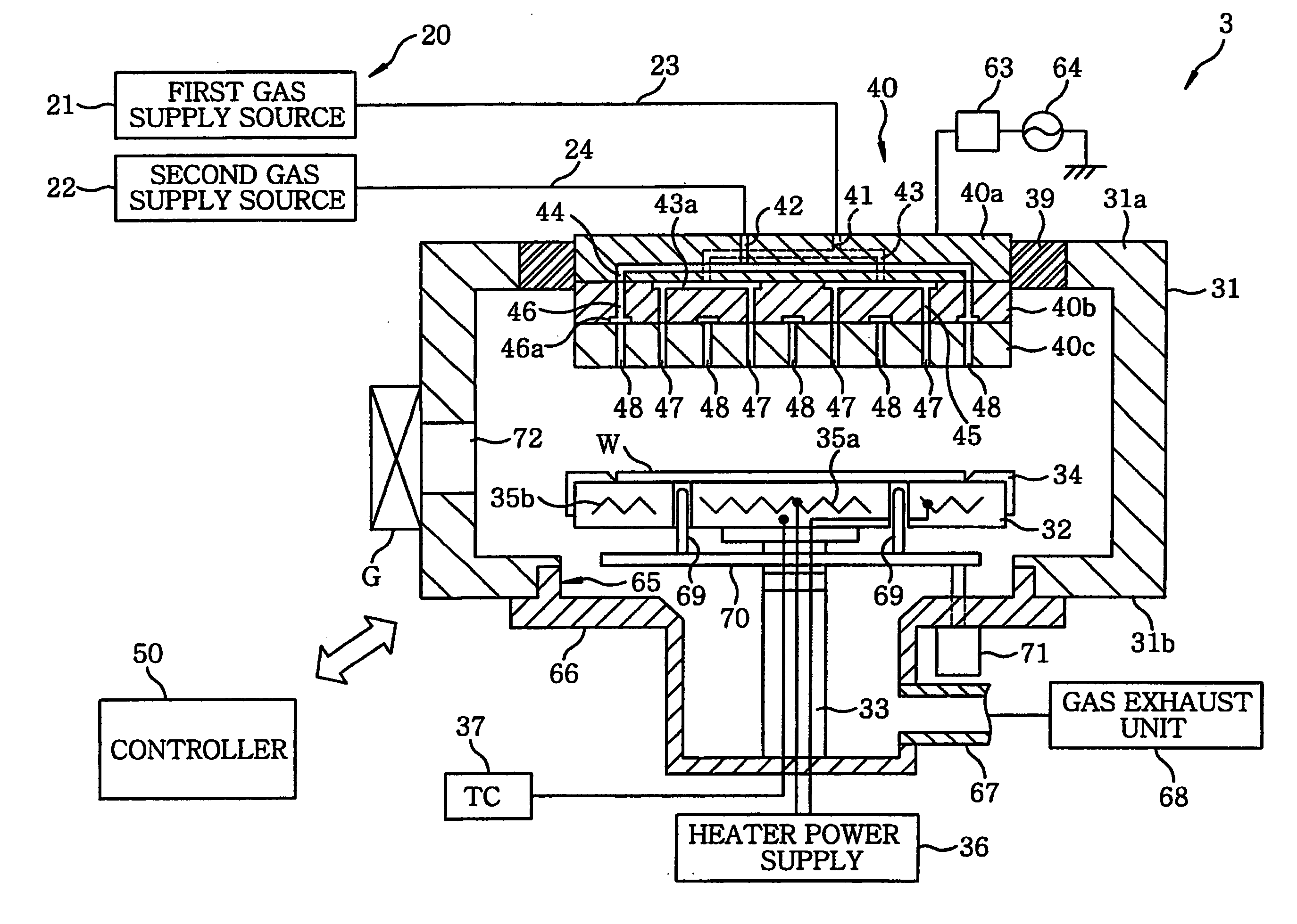
[0048]FIG. 4 is a schematic configuration view of a multi-chamber type film forming system for performing a TiN film forming method as an example of a substrate processing method in accordance with the present invention.

[0049] As shown in FIG. 4, the film forming system 100 includes four film forming apparatuses: two Ti film forming apparatuses 1 and 2 for forming a Ti film on a wafer W by employing a CVD method and two TiN film forming apparatuses 3 and 4 for forming a TiN film on a wafer W. The film forming apparatuses 1 to 4 are disposed to correspond to four sides of a hexagonal wafer transfer chamber 5. Further, load lock chambers 6 and 7 are disposed at the remaining two sides of the wafer transfer chamber 5, and a wafer loading / unloading chamber 8 is connected to the load lock chambers 6 and 7 at the opposite side with respect to the wafer transfe...


PUM

PropertyMeasurementUnit
temperatureaaaaaaaaaa
temperaturesaaaaaaaaaa

Abstract

Disclosed is a substrate processing method wherein the infrared absorptance or infrared transmittance of a substrate to be processed is measured in advance, and the substrate is processed according to the measured value while independently controlling temperatures at least in a first region located in the central part of the substrate and in a second region around the first region using temperature control means which are respectively provided for the first region and the second region and can be controlled independently from each other.

Description

FIELD OF THE INVENTION [0001] The present invention relates to a substrate processing method and a substrate processing apparatus; and, more particularly, to a substrate processing method and a substrate processing apparatus for performing, e.g., a film forming process on a target substrate such as a semiconductor wafer. BACKGROUND OF THE INVENTION [0002] In a film forming process performed in manufacturing various semiconductor devices, a temperature control is vital to secure a desired characteristic of a thin film and a high precision in film thickness. Any problem in the temperature control can directly lead to deterioration of the quality or reliability of final semiconductor devices. [0003] A film forming apparatus for forming a film on a semiconductor wafer (hereinafter, also referred to as “wafer”) as a substrate to be processed by employing, e.g., a CVD method includes a susceptor serving as a substrate mounting table for mounting the wafer thereon, wherein the susceptor is...

Claims


Application Information

Patent Timeline
Patent Type & Authority Applications(United States)
IPC IPC(8): C23C16/46H01L21/02H01L21/285
CPCC23C16/46H01L22/10H01L21/67248C23C16/52H01L21/02
Inventor TADA, KUNIHIROMIYASHITA, HIROYUKIGUNJI, ISAO
Owner TOKYO ELECTRON LTD
Why Eureka
Try Eureka