
Manufacturing method of wiring substrate

a manufacturing method and wiring technology, applied in the direction of manufacturing tools, soldering apparatus, other domestic objects, etc., can solve the problems of increasing the number of steps the complexity of the manufacturing step of the wiring substrate, so as to achieve the effect of easy formation of a solder layer

Inactive Publication Date: 2007-12-20
SHINKO ELECTRIC IND CO LTD
View PDF4 Cites 12 Cited by
  • Summary
  • Abstract
  • Description
  • Claims
  • Application Information

AI Technical Summary

Benefits of technology

[0013]Exemplary embodiments of the present invention provide a manufacturing method of a wiring substrate capable of easily forming a solder layer on only a surface of a flip chip pad in a substrate on which the flip chip pad and a bonding pad are juxtaposed.
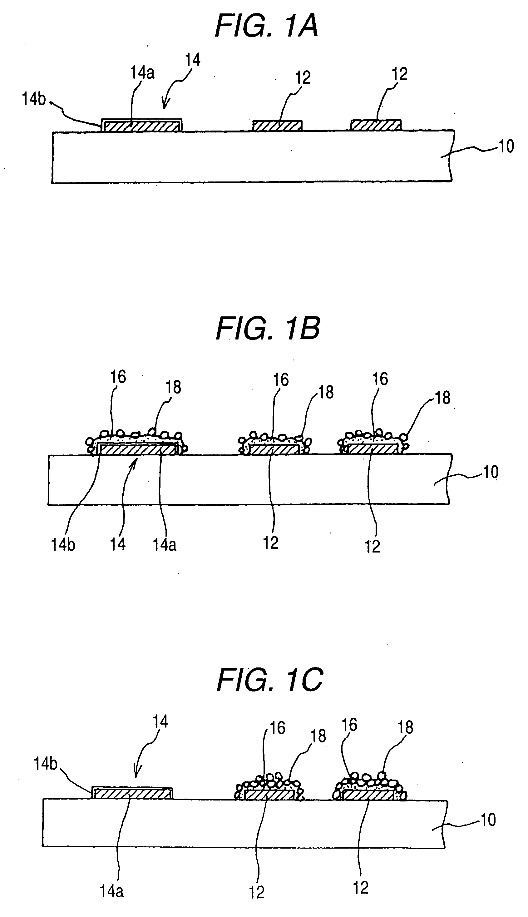
[0016]In such an exemplary embodiment of the preset invention, each of the pH values of the first adhesive treatment liquid and the second adhesive treatment liquid is adjusted in the range of 4 to 6 and in that case, the pH value of the second adhesive treatment liquid is adjusted so as to become higher than the pH value of the first adhesive treatment liquid. Particularly, the pH value of the second adhesive treatment liquid is adjusted so as to become higher than the pH value of the first adhesive treatment liquid by 0.5 or more. Therefore, an adhesive layer with a sufficient film thickness can be formed on a metal surface of a flip chip pad and sufficient solder powder can be attached and also, the solder powder can be prevented from attaching to a metal surface of a bonding pad.
[0019]One or more embodiments of the present invention may include one or more the following advantages. For example,in the exemplary embodiment of the present invention, an adhesive layer formed on a metal surface of a bonding pad among the adhesive layers formed on both surfaces of a flip chip pad and the bonding pad by immersion-treating a substrate with a first adhesive treatment liquid is peeled from the metal surface of the bonding pad in the case of immersion-treating this substrate with a second adhesive treatment liquid, and the metal surface of the bonding pad can be exposed.
[0021]According to such an exemplary embodiment of the present invention, there is no need to cover the bonding pad with a mask plate and a step of mounting to and demounting from the mask plate can be omitted and a manufacturing step of a wiring substrate can be simplified.
[0022]Further, according to the exemplary embodiment of the present invention, a step of immersion-treating the substrate with the adhesive treatment liquid and attaching the solder powder to the adhesive layer formed on the flip chip pad is performed at least two times, so that sufficient solder powder can be attached to the flip chip pad and a film thickness of a solder layer formed finally can be thickened. As a result of this, when flip chip connection between a semiconductor element and the obtained wiring substrate is made, the semiconductor element can surely be connected to the wiring substrate and reliability of a semiconductor apparatus obtained finally can be improved.

Problems solved by technology

However, covering the noble metal surface of the bonding pad 104 with the mask plate 200 results in an increase in the number of steps of a manufacturing step of the wiring substrate and the manufacturing step of the wiring substrate becomes complicated.

Method used


Image

  • Manufacturing method of wiring substrate
  • Manufacturing method of wiring substrate
  • Manufacturing method of wiring substrate

Examples


example 1

[0052]A substrate 10 shown in FIG. 1A was prepared. Flip chip pads 12, 12 . . . and a bonding pad 14 are formed on the same surface of this substrate 10. This flip chip pad 12 is formed by copper. Also, in the bonding pad 14, a body part 14a made of copper is covered with a plated layer 14b made by forming a gold plated layer on a nickel plated layer used as an underlaying plated layer.

[0053]Further, a first adhesive treatment liquid in which a pH value of SJ-CH1000 (trade name) manufactured by Showa Denko K.K. used as an adhesive treatment liquid was adjusted to 4 to 4.5 and a second adhesive treatment liquid adjusted to a pH value higher than the pH value of the first adhesive treatment liquid by 0.5 were prepared.

[0054]Then, after the substrate 10 was immersion-treated with the first adhesive treatment liquid and the substrate 10 taken out of the first adhesive treatment liquid was sprinkled with solder powder with the average particle size of 7 μm, the extra solder powder was sh...

example 2

[0060]Sprinkling treatment of solder powder and immersion-treatment of a substrate 10 with an adhesive treatment liquid were performed in a manner similar to Example 1 except that solder powder with the average particle size of 7 μm was used as solder powder sprinkled on the substrate 10 after immersion-treatment with the first adhesive treatment liquid and solder powder with the average particle size of 5.5 μm was used as solder powder sprinkled on the substrate 10 after immersion-treatment with the second adhesive treatment liquid in Example 1.

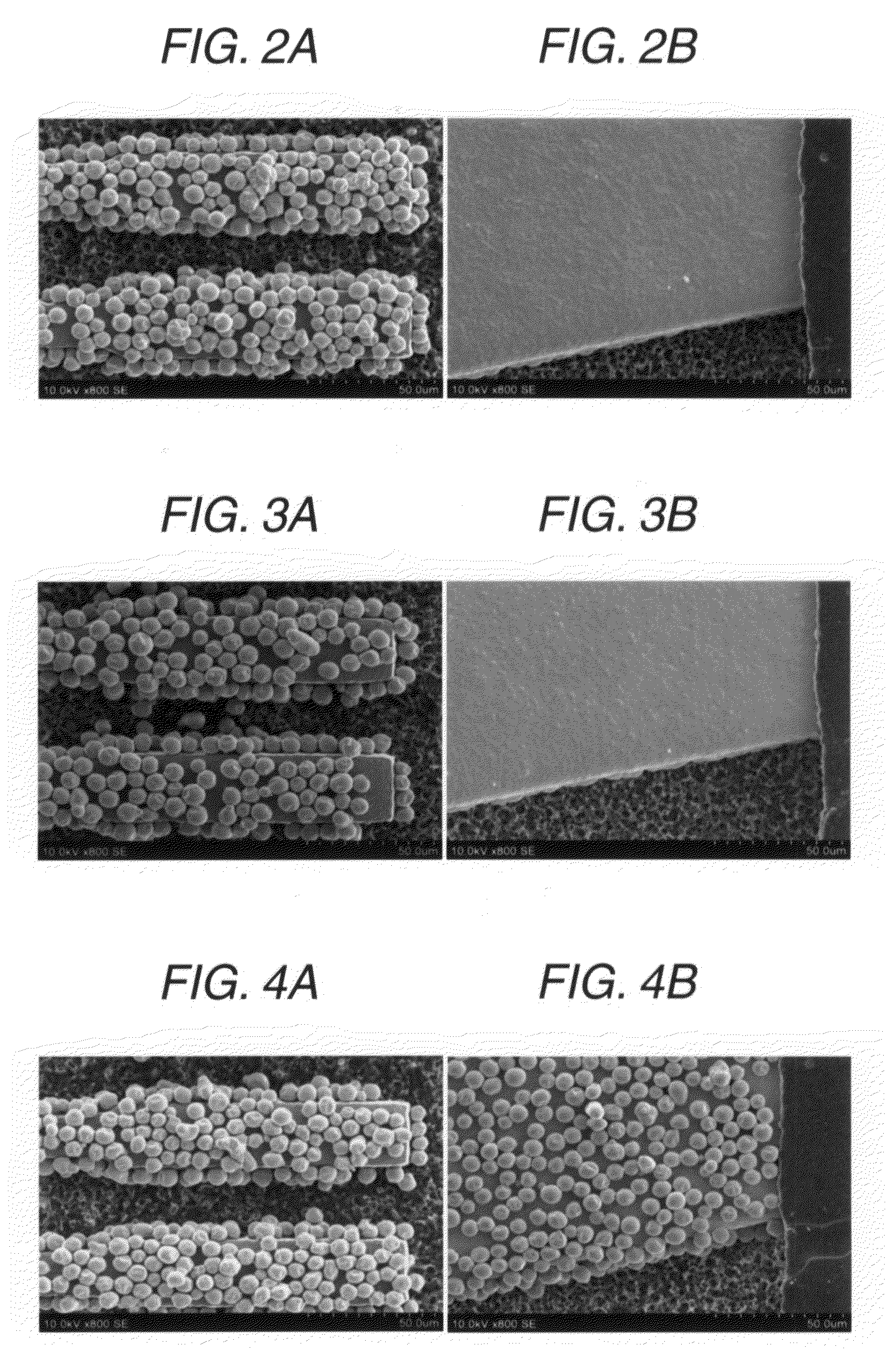
[0061]FIGS. 3A, 3B show electron microscope photographs of a flip chip pad 12 and a bonding pad 14 of the substrate 10 in which a step of sprinkling the substrate with the solder powder after immersion-treating the substrate 10 with the adhesive treatment liquid was performed two times in this manner. FIG. 3A is the photograph for the flip chip pad 12, and FIG. 3B is the photograph for the bonding pad 14.

[0062]As is evident from FIGS. 3A, 3B...

example 3

[0078]Sprinkling treatment of solder powder and immersion-treatment of a substrate 10 with an adhesive treatment liquid were performed in a manner similar to Example 1 except that each of the pH values of the first adhesive treatment liquid and the second adhesive treatment liquid was changed as shown in the following Table 1 in Example 1.

[0079]With respect to the substrate 10 in which a series of treatment was ended, a state of attachment of the solder powder to a substrate surface, a flip chip pad 12 and a bonding pad 14 was visually observed and its evaluation result was together shown in Table 1.

TABLE 1FirstSecondadhesiveadhesivetreatmenttreatmentSubstrateFlip chipNo.liquidliquidsurfacepadBonding pad14.3+1.0◯◯◯25.5+0.5◯◯◯35.0+0.5◯Δ (Note 2)◯44.0+0.2◯◯Δ~X (Note3)Note 1)◯; Solder powder does not attach to a substrate surface and a bonding pad, and sufficient solder powder attaches to a flip chip pad.Δ; Acceptable though there is some problem.X; RejectionNote 2)Acceptable though th...


PUM

PropertyMeasurementUnit
particle sizeaaaaaaaaaa
thicknessaaaaaaaaaa
particle sizeaaaaaaaaaa

Abstract

A bonding pad and flip chip pads in which the surfaces are formed by different metals are juxtaposed on a substrate. The substrate is immersion-treated with a first adhesive treatment liquid which contains an adhesive giving compound for reacting with only a metal surface and giving adhesion properties and is adjusted to a pH value for forming adhesive layers on both of the metal surfaces of the flip chip pads and the bonding pad. Solder powder is attached to the adhesive layers formed on each of the metal surfaces of the pads. Then, the substrate is again immersion-treated with a second adhesive treatment liquid which contains an adhesive giving compound for reacting with only a metal surface and giving adhesion properties and is adjusted to a pH value for forming the adhesive layers on the metal surfaces of the flip chip pads while peeling the adhesive layer of the metal surface of the bonding pad. Subsequently, the solder powder attached to only the flip chip pads is melted by performing reflow after the solder powder is attached to the adhesive layers formed on only the flip chip pads.

Description

[0001]This application claims priority to Japanese Patent Application No. 2006-169981, filed Jun. 20, 2006, in the Japanese Patent Office. The priority application is incorporated by reference in its entirety.TECHNICAL FIELD[0002]The present disclosure relates to a manufacturing method of a wiring substrate, and relates to a manufacturing method of a wiring substrate on which a bonding pad for wire bonding connection and a flip chip pad for flip chip connection in which solder is deposited on a surface are juxtaposed.RELATED ART[0003]In a wiring substrate on which flip chip connection of a semiconductor element is made, flip chip pads 102, 102 . . . for flip chip connection and a bonding pad 104 for wire bonding connection may be juxtaposed on one surface of a substrate 100 as shown in FIG. 8.[0004]A solder layer for fastening an electrode terminal of the abutting semiconductor element is formed in such flip chip pads 102, 102 . . . and a surface of the bonding pad 104 for wire bond...

Claims


Application Information

Patent Timeline
Patent Type & Authority Applications(United States)
IPC IPC(8): H01L21/00
CPCH01L21/4846Y10T29/49144H01L24/16H01L24/48H01L2224/16H01L2224/48227H01L2224/85439H01L2224/85444H01L2224/85447H01L2224/85464H01L2924/01046H01L2924/01078H01L2924/01079H05K3/243H05K3/3484H05K2201/0391H05K2203/0425H05K2203/124H01L2924/01019Y10T29/49405Y10T29/49142H01L21/6835H01L2924/00014H05K3/3485H01L2224/45099H01L2224/45015H01L2924/207H05K3/34
Inventor NAKABAYASHI, YOKO
Owner SHINKO ELECTRIC IND CO LTD
Learn More