Gallium nitride material devices and methods of forming the same

a gallium nitride and silicon substrate technology, applied in the field of silicon substrate can solve the problems of presenting challenges in the process of forming gallium nitride materials on silicon substrates to produce semiconductor devices

Inactive Publication Date: 2007-12-27
NITRONEX
View PDF55 Cites 114 Cited by
  • Summary
  • Abstract
  • Description
  • Claims
  • Application Information

AI Technical Summary

Problems solved by technology

However, forming gallium nitride materials on silicon substrates to produce semiconductor devices presents challenges which arise from differences in the lattice constant, thermal expansion, and band gap between silicon and gallium nitride.

Method used


Image

  • Gallium nitride material devices and methods of forming the same
  • Gallium nitride material devices and methods of forming the same
  • Gallium nitride material devices and methods of forming the same

Examples


Embodiment Construction

[0046] The invention provides gallium nitride material structures, devices and methods of forming the structures and devices.

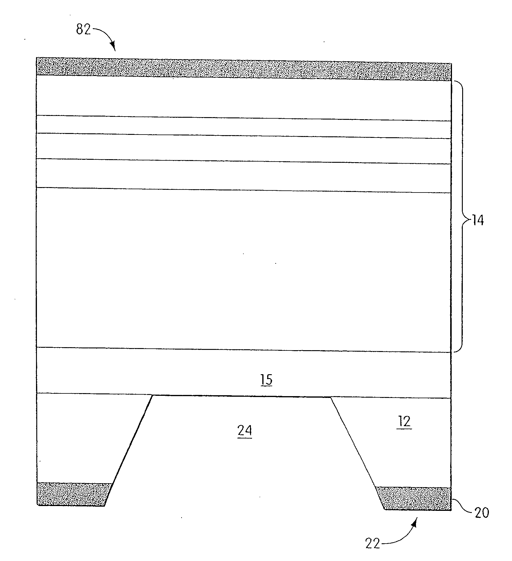
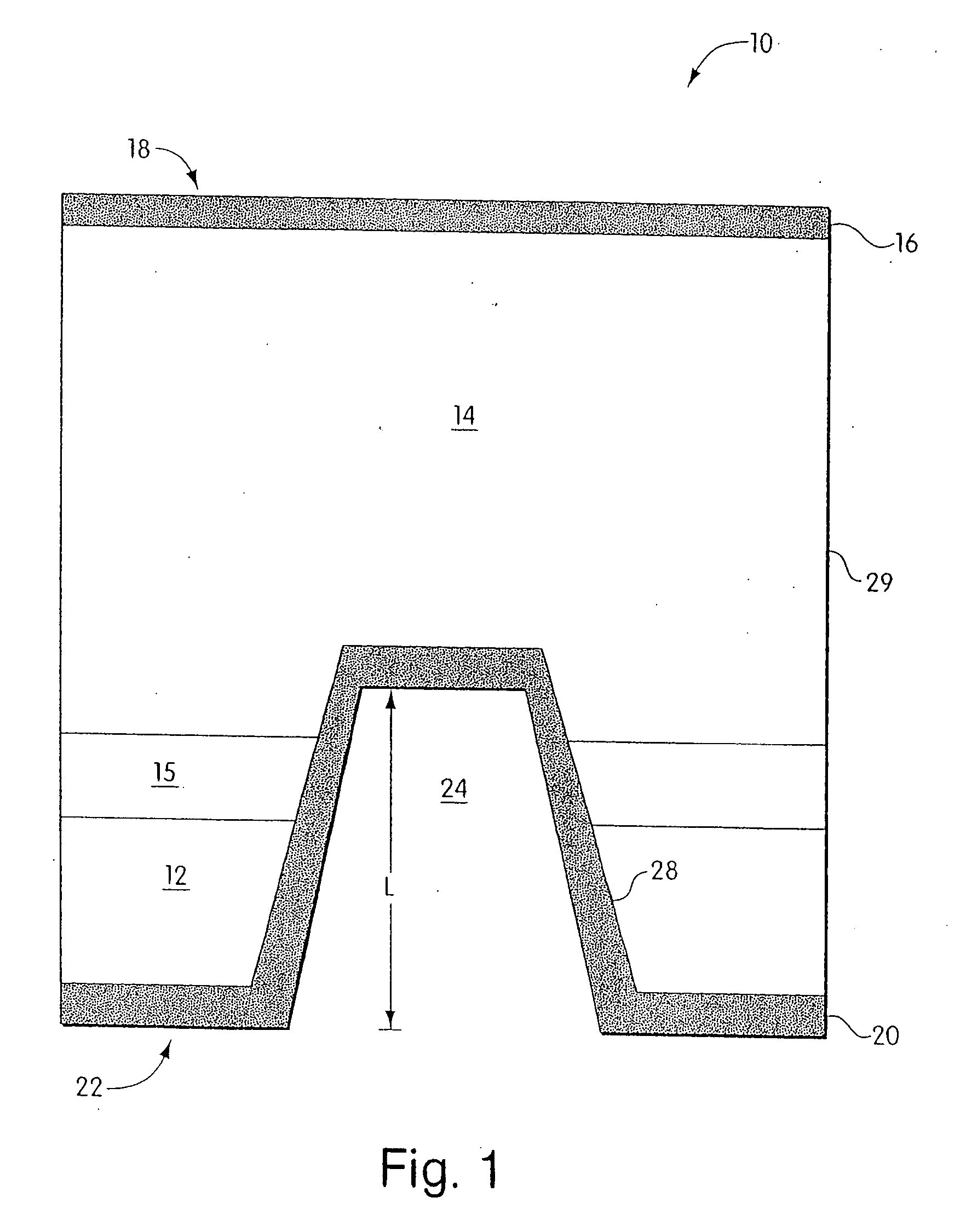
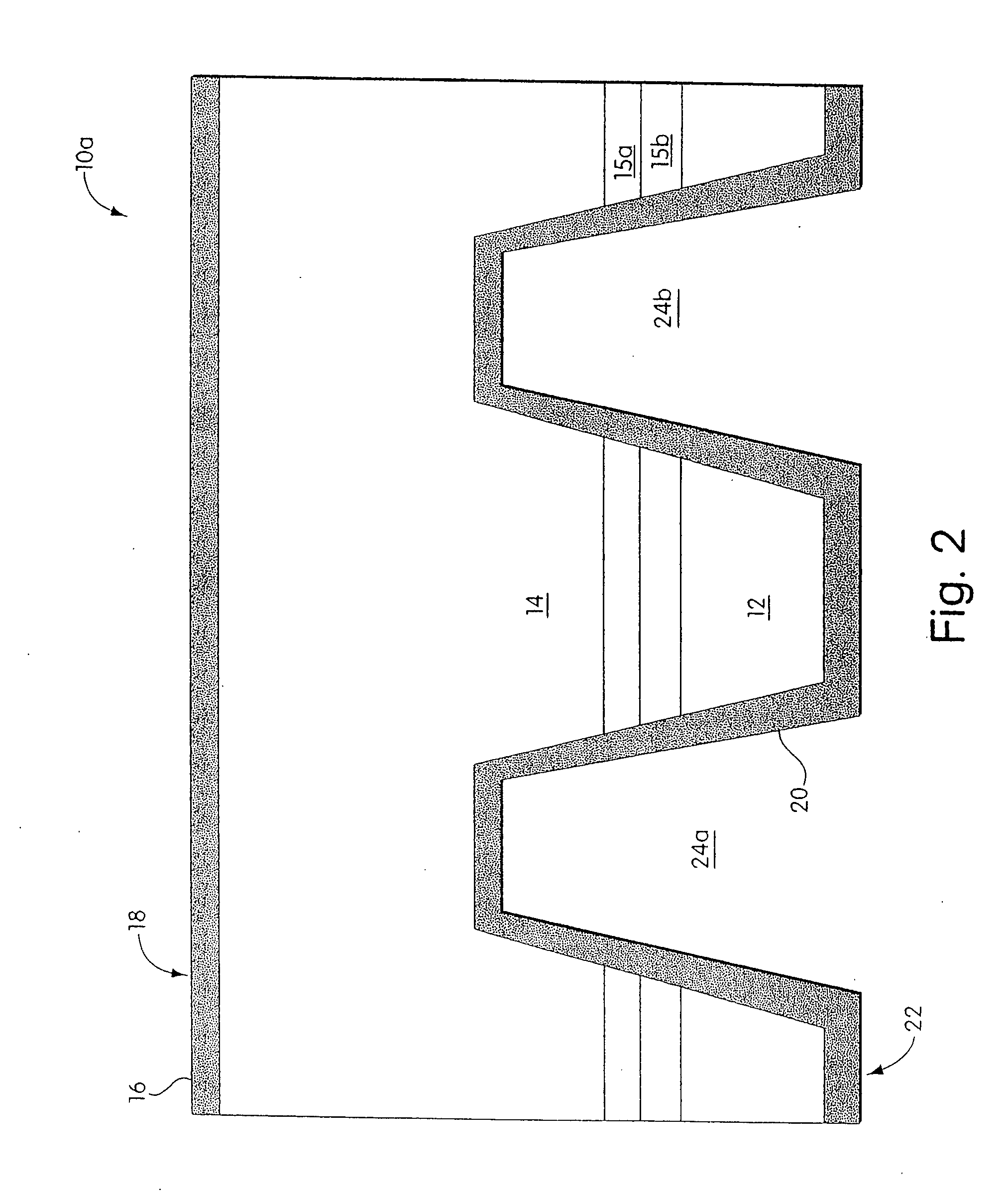
[0047] Referring to FIG. 1, a semiconductor device 10 according to one embodiment of the invention is shown. Semiconductor device 10 includes a substrate 12 and a gallium nitride material device region 14 formed over the substrate. As described further below, device structures are typically formed, at least in part, within gallium nitride material region 14. Device 10 further includes a transition layer 15 formed on substrate 12, for example, to facilitate the subsequent deposition of gallium nitride material device region 14. In some cases, the transition layer (or, at least a portion of the transition layer) may be non-conducting. A topside electrical contact 16 (on a topside 18 of the device) and a backside electrical contact 20 (on a backside 22 of the device) are provided for connection to an external power supply that powers the device. Backside contact...


PUM

PropertyMeasurementUnit
diametersaaaaaaaaaa
diametersaaaaaaaaaa
diametersaaaaaaaaaa

Abstract

The invention provides gallium nitride material devices, structures and methods of forming the same. The devices include a gallium nitride material formed over a substrate, such as silicon. Exemplary devices include light emitting devices (e.g., LED's, lasers), light detecting devices (such as detectors and sensors), power rectifier diodes and FETs (e.g., HFETs), amongst others.

Description

RELATED APPLICATIONS [0001] This application is a continuation of U.S. patent application Ser. No. 10 / 650,122, filed Aug. 25, 2003, and entitled “Gallium Nitride Material Devices and Methods of Forming the Same”, which is a continuation-in-part of U.S. patent application Ser. No. 09 / 792,414 (now U.S. Pat. No. 6,611,002), filed Feb. 23, 2001, and entitled “Gallium Nitride Material Devices and Methods Including Backside Vias”. All of the above-mentioned disclosures are incorporated herein by reference.FIELD OF INVENTION [0002] The invention relates generally to semiconductor materials and, more particularly, to gallium nitride materials and methods of producing gallium nitride materials. BACKGROUND OF INVENTION [0003] Gallium nitride materials include gallium nitride (GaN) and its alloys such as aluminum gallium nitride (AlGaN), indium gallium nitride (InGaN), and aluminum indium gallium nitride (AlInGaN). These materials are semiconductor compounds that have a relatively wide, direct...

Claims


Application Information

Patent Timeline
Patent Type & Authority Applications(United States)
IPC IPC(8): H01L33/00H01L21/28H01L21/338H01L29/06H01L29/20H01L29/417H01L29/47H01L29/80H01L29/812H01L29/861H01L29/872H01L33/20H01L33/32H01L33/38H01L47/02H01S5/343
CPCH01L29/0657Y02E10/544H01L29/417H01L29/66204H01L29/66462H01L29/802H01L29/861H01L31/03044H01L31/03048H01L31/1848H01L31/1856H01L33/007H01L33/0079H01L33/20H01L33/32H01L33/38H01L33/382H01L47/026H01S5/0425H01L29/2003H01L2924/10155H01L29/7786H01S5/04254H01S5/0207H01S5/32341H01L33/0093H10N80/107
Inventor WEEKS, T. WARREN JR.LINTHICUM, KEVIN J.
Owner NITRONEX
Why Eureka
Try Eureka