Transient voltage suppression device

a transient voltage and suppression device technology, applied in semiconductor devices, diodes, electrical devices, etc., can solve the problems of disadvantageous rise of clamping voltage of prior art tv devices, difficult to achieve clamping voltage, etc., and achieve the effect of low clamping voltag

Inactive Publication Date: 2005-03-15
PROTEK DEVICES
View PDF6 Cites 55 Cited by
  • Summary
  • Abstract
  • Description
  • Claims
  • Application Information

AI Technical Summary

Benefits of technology

It is therefore an object of the present invention to provide a flip chip that overcomes the disadvantages of the prior art, a

Problems solved by technology

As operating frequencies become higher, the internal capacitance of the avalanche diode becomes problematic.
The clamping voltage of a prior art T

Method used


Image

  • Transient voltage suppression device
  • Transient voltage suppression device
  • Transient voltage suppression device

Examples


Embodiment Construction

The embodiments discussed below are only examples of the many advantageous uses of the innovative teachings herein. In general, statements made in the specification of the present application do not necessarily limit any of the various claimed inventions. Moreover, some statements may apply to some inventive features but not to others. In general, unless otherwise indicated, singular elements may be in the plural and vice versa with no loss of generality, e.g., one die, two die. The terms first, second, and the like, in the description and in the claims, if any, are used for distinguishing between similar elements and not necessarily for describing a sequential or chronological order. The terms top, front, side, and the like, in the description and in the claims, if any, are used for descriptive purposes and not necessarily for describing relative positions.

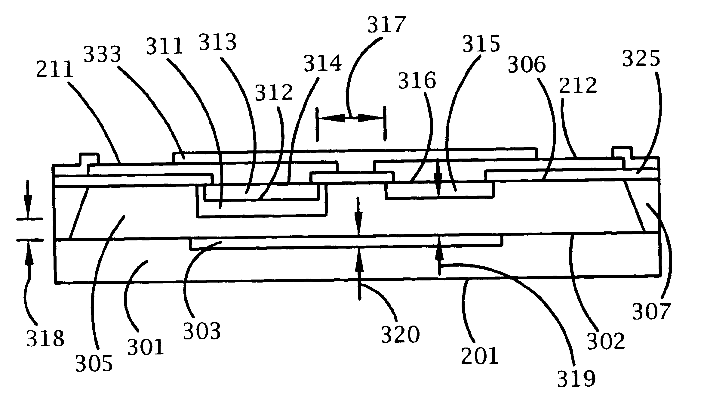
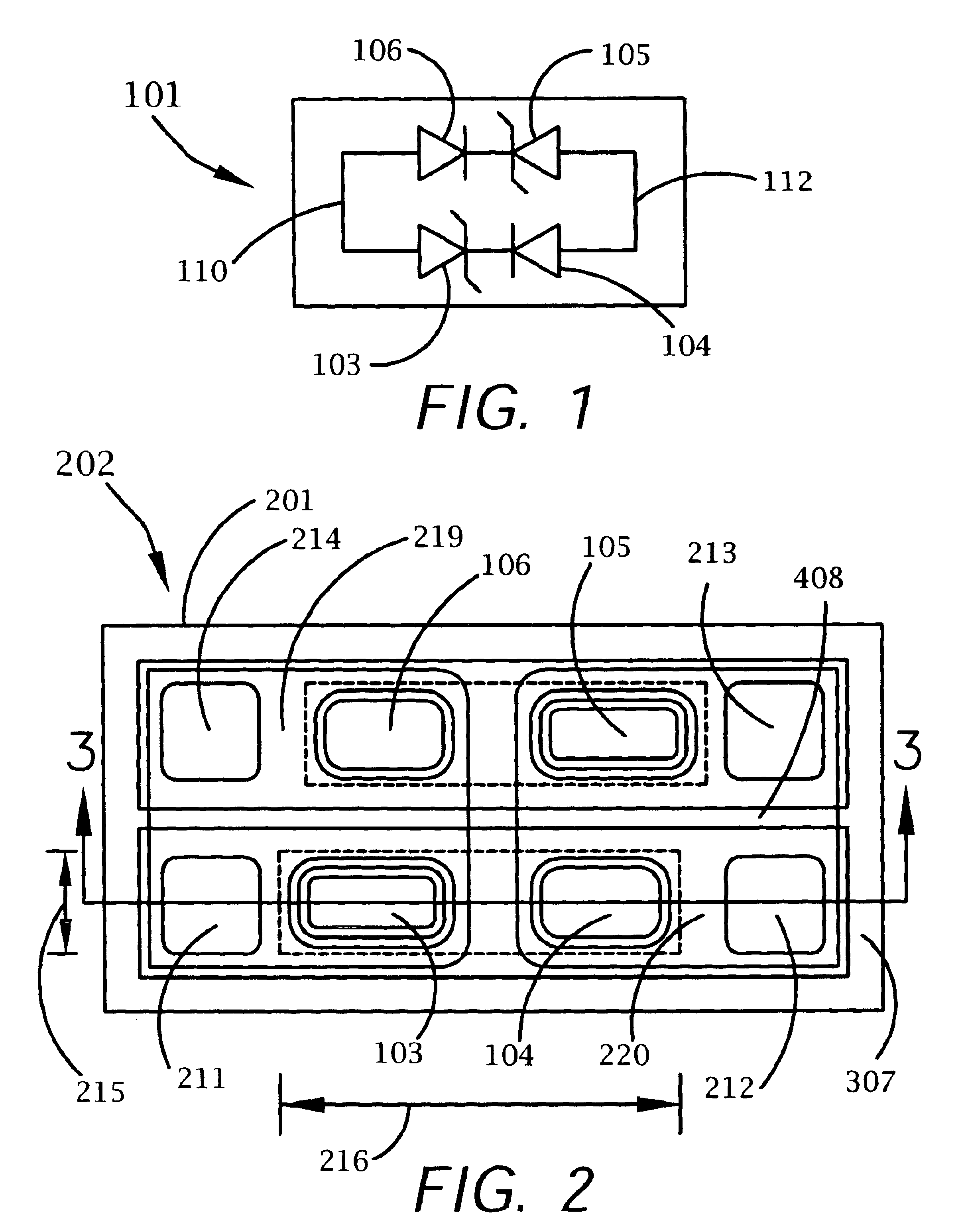
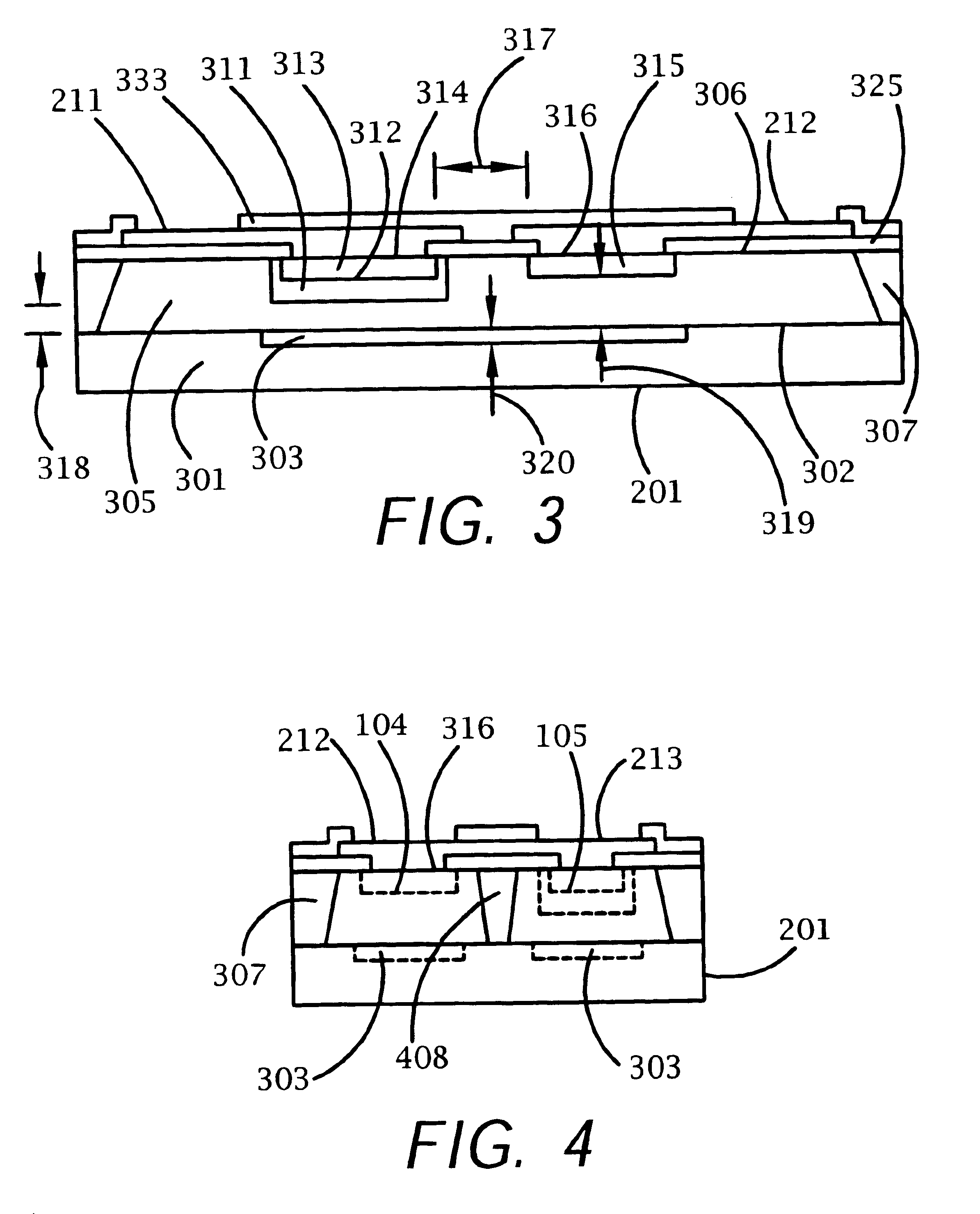
FIG. 1 is a schematic electrical diagram of a TVS device 101 in accordance with the invention. The TVS device 101 comprises a f...


PUM


Abstract

A bi-directional transient voltage suppression (“TVS”) device (101) includes a semiconductor die (201) that has a first avalanche diode (103) in series with a first rectifier diode (104) connected cathode to cathode, electrically coupled in an anti-parallel configuration with a second avalanche diode (105) in series with a second rectifier diode (106) also connected cathode to cathode. All the diodes of the TVS device are on a single semiconductor substrate (301). The die has a low resistivity buried diffused layer (303) having a first conductivity type disposed between a semiconductor substrate (301) having the opposite conductivity type and a high resistivity epitaxial layer (305) having the first conductivity type. The buried diffused layer shunts most of a transient current away from a portion of the epitaxial layer between the first avalanche diode and the first rectifier diode, thereby reducing the clamping voltage relative to the breakdown voltage. The TVS device is packaged as a flip chip (202) that has four solder bump pads (211-214). The abstract is submitted with the understanding that it will not be used to interpret or limit the scope or meaning of the claims pursuant to 37 C.F.R. §1.72(b).

Description

BACKGROUND OF THE INVENTION1. Field of the InventionThis invention relates generally to active solid-state devices, and more particularly to a transient voltage suppression device having one or more avalanche diodes.2. Description of the Related ArtTransient voltage suppression (“TVS”) devices comprising an avalanche diode are well known. As the reverse avalanche voltage is made smaller, a depletion region of the avalanche diode narrows, resulting in a higher internal capacitance of the avalanche diode. As operating frequencies become higher, the internal capacitance of the avalanche diode becomes problematic. A known solution to the capacitance problem is to add a rectifier diode in series with the avalanche diode, with either the anodes or the cathodes of the diodes connected together. A rectifier diode has a smaller capacitance than an avalanche diode, and the total capacitance of a pair of such diodes in series is less than the sum of the two capacitances.TVS devices having both...

Claims


Application Information

Patent Timeline
IPC IPC(8): H01L29/66H01L29/866H01L27/08H01L29/861
CPCH01L27/0814H01L29/866H01L29/861H01L27/0817
Inventor MATTESON, FREDPAI, VENKATESH PANEMANGALORECARTMELL, DONALD K.
Owner PROTEK DEVICES
Why Eureka
Try Eureka