
Semiconductor device

Active Publication Date: 2007-12-27
RENESAS ELECTRONICS CORP
View PDF4 Cites 46 Cited by
  • Summary
  • Abstract
  • Description
  • Claims
  • Application Information

AI Technical Summary

Benefits of technology

[0011]Advantageous effects obtained by a representative one of the inventions disclosed in the present application will be described briefly as follows:
[0012]In a nonvolatile memory cell having a data read transistor, a capacitive element and a data write / erase element, the data read transistor and the data write / erase element are disposed away from each other by the capacitive element disposed therebetween. A first electrode of the capacitive element, a second electrode of the data read transistor and a third electrode of the data write / erase element are constituted of part of a common floating gate electrode extending along the direction in which the data read transistor, the capacitive element and the data write / erase element are arranged. The second electrode of the data read transistor and the third electrode of the data write / erase element are spaced away from each other by the first electrode of the capacitive element disposed therebetween. Thus, the area of a nonvolatile memory circuit section provided in a semiconductor device can be reduced.

Problems solved by technology

However, there has recently been a tendency that the memory capacity of the nonvolatile memory circuit section provided in the semiconductor device also increases.
Therefore, an important problem is how to reduce the occupied area of the nonvolatile memory circuit section while larger memory capacity is being ensured, in such a manner that the area of laying out the nonvolatile memory circuit section does not bring pressure to bear on the area of laying out a main circuit.

Method used


Image

  • Semiconductor device
  • Semiconductor device
  • Semiconductor device

Examples


first preferred embodiment

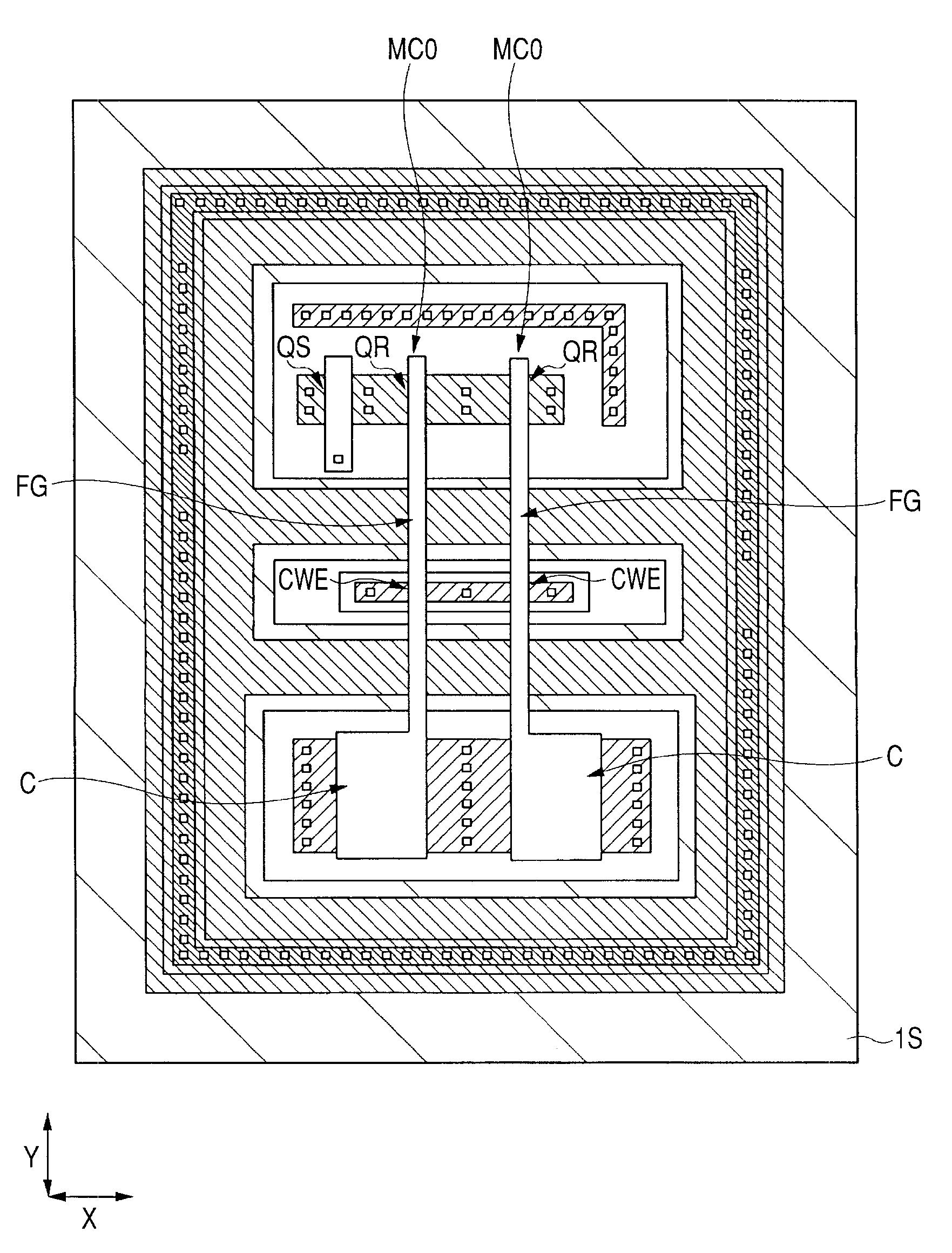
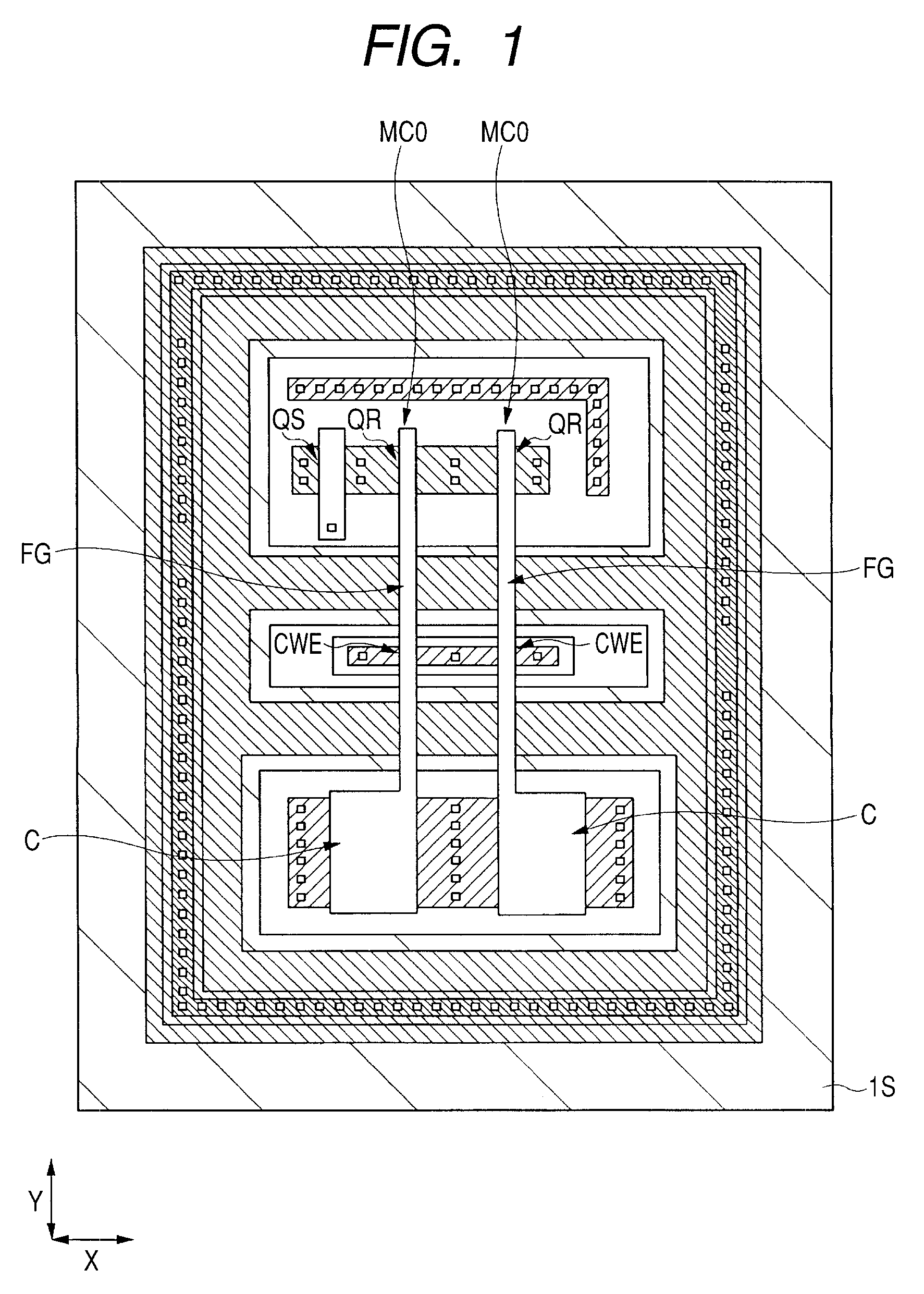
[0072]FIG. 1 shows a plan view of memory cells MC0 corresponding to one bit of a flash memory suitable for a semiconductor device discussed by the present inventors. Incidentally, although FIG. 1 is a plan view, parts thereof are hatched to make it easy to see the drawing. A symbol Y is a first direction and indicates the direction in which local data lines extend. A symbol X is a second direction orthogonal to the first direction Y and indicates the direction in which word lines extend.

[0073]In the present configuration, the two memory cells MC0 are arranged for one bit (one bit / two cell configuration). One selection MIS•FET (Metal Insulator Semiconductor Field Effect Transistor) QS is arranged for one bit. Each of the memory cells MC0 has a data read MIS•FETQR that shares a floating gate electrode FG, a data write / erase charge injection / discharge part or section CWE and a capacitance part or section C. The data read MIS•FETQR, the data write / erase charge injection / discharge sectio...

second preferred embodiment

[0197]A second embodiment is different from the first embodiment in the following configurations in particular.

[0198]The first is that the configurations of a pair of semiconductor regions for source / drain, of a data read MIS•FET of each memory cell are identical to the configurations (including the p-type hollow regions) of the pair of semiconductor regions for source / drain, of the n channel type MIS•FET of the low breakdown section (1.5V device) in the main circuit.

[0199]The second is that the gate length of each data write / erase charge injection / discharge section of the memory cell is made short, and part of a p-type semiconductor region of the charge injection / discharge section is caused to extend (diffuse into) to a surface layer of a substrate placed directly below a capacitive electrode.

[0200]The third is that p-type wells of the charge injection / discharge sections adjacent to each other are separated by n+-type semiconductor regions (each corresponding to an n+-type diffusio...

third preferred embodiment

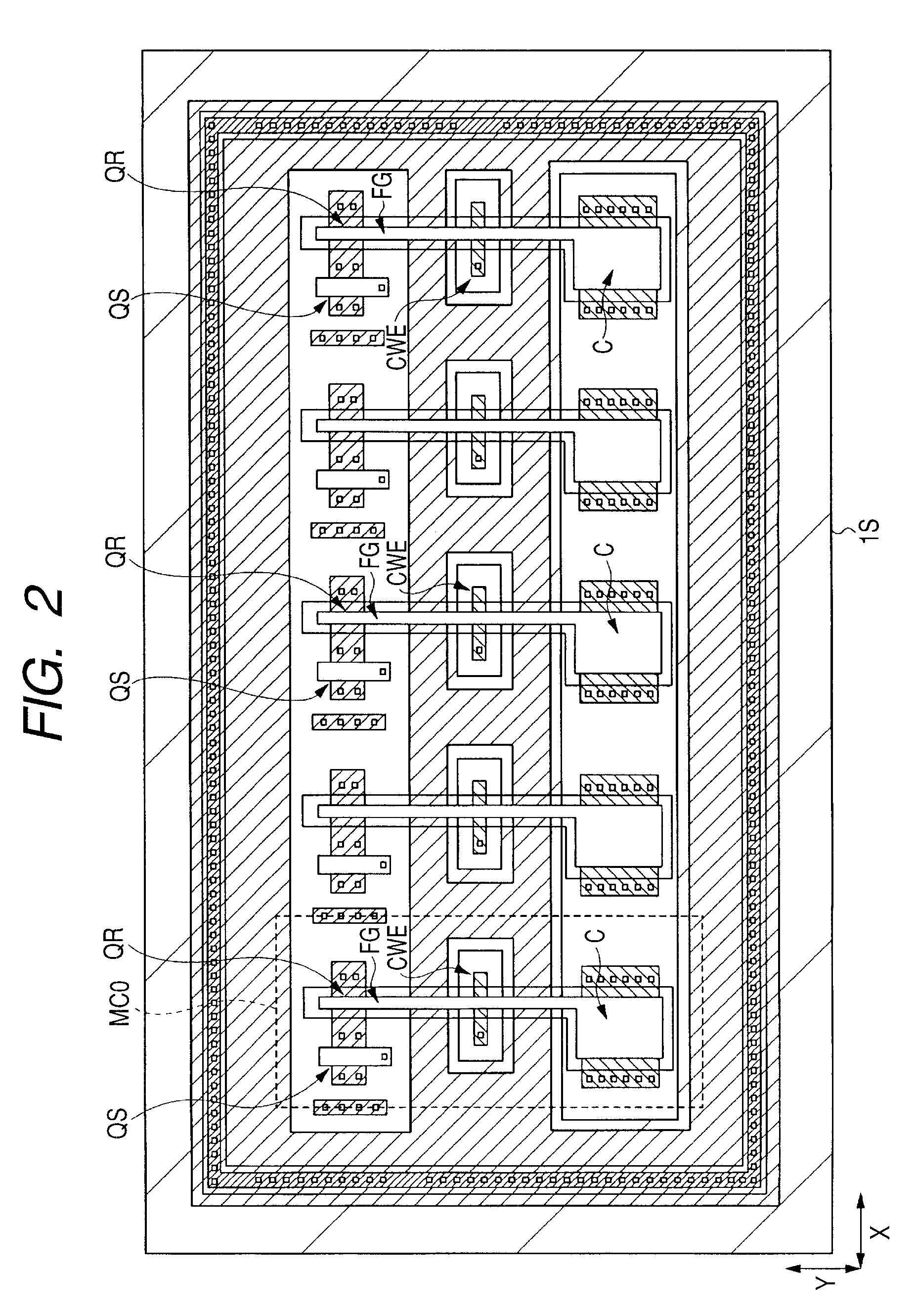
[0246]FIG. 43 shows a plan view of a flash memory for a semiconductor device according to a third embodiment, FIG. 44 shows a fragmentary enlarged plan view of the flash memory shown in FIG. 43, and FIG. 45 shows a cross-sectional view taken along line Y3-Y3 of FIG. 43, respectively. Incidentally, although FIGS. 43 and 44 are plan views, parts thereof are hatched to make it easy to see the drawings. Cross-sectional views taken along lines X1-X1, X2-X2 and X3-X3 of FIG. 44 are respectively identical to FIGS. 22, 7 and 24.

[0247]In the third embodiment, the length (gate length) in a second direction X, of a capacitive electrode FGC1 of each charge injection / discharge section CWE is longer than the length (gate length) in the second direction X, of each data read MIS•FETQR. In the third embodiment, constitutions other than it are identical to those described in the first and second embodiments.

[0248]Thus, in the third embodiment, the length in the second direction X, of a second portion...


PUM


Abstract

p-type wells are provided within an n-type embedded well of a semiconductor substrate lying in an area for forming a flash memory, in a state of being isolated from one another. A capacitance section, a data write / erase charge injection / discharge section and a data read MIS•FET are disposed in each of the p-type wells. The capacitance section is disposed between the data write / erase charge injection / discharge section and the data read MIS•FET. In the data write / erase charge injection / discharge section, writing and erasing of data by an FN tunnel current at a channel entire surface are performed.

Description

CROSS-REFERENCE TO RELATED APPLICATIONS[0001]The disclosure of Japanese patent application No. 2006-172115 filed on Jun. 22, 2006 including the specification, drawings and abstract is incorporated herein by reference in its entirety.BACKGROUND OF THE INVENTION[0002]The present invention relates to a semiconductor device technique, and particularly to a technique effective when applied to a semiconductor device having a nonvolatile memory circuit section.[0003]Of semiconductor devices, there is known one that has thereinside a nonvolatile memory circuit section for storing relatively small-capacity information such as information used upon trimming, relief and image adjustments of an LCD (Liquid Crystal Device), information about the production number of a semiconductor device, etc.[0004]This semiconductor device having the nonvolatile memory circuit section has been described in, for example, Japanese Unexamined Patent Publication No. 2006-80247 (refer to a patent document 1). The f...

Claims


Application Information

Patent Timeline
IPC IPC(8): H01L29/788
CPCG11C16/0441H01L27/0207H01L27/0629H01L27/11558H01L27/11519H01L27/11521H01L27/11526H01L27/105H10B41/10H10B41/40H10B41/60H10B41/30
Inventor SHIBA, KAZUYOSHIOKA, YASUSHI
Owner RENESAS ELECTRONICS CORP
Features
  • Generate Ideas
  • Intellectual Property
  • Life Sciences
  • Materials
  • Tech Scout
  • Unparalleled Data Quality
  • Higher Quality Content
  • 60% Fewer Hallucinations
Learn More