Active ESD Protection

a technology of active esd and protection, which is applied in the direction of emergency protective arrangements for limiting excess voltage/current, electrical equipment, and semiconductor devices, can solve problems affecting the failure point of the circuit, and achieve the effects of reducing the voltage stress on each, increasing the failure voltage, and increasing the failure voltag

Inactive Publication Date: 2007-12-27
IBM CORP
View PDF11 Cites 24 Cited by
  • Summary
  • Abstract
  • Description
  • Claims
  • Application Information

AI Technical Summary

Benefits of technology

[0007]In analyzing the problems described above, it has been observed that the state of the circuit when it is powered up by an ESD event can affect the failure point of the circuit. Certain states will increase the failure voltage by causing the voltage on the chip pad to be distributed among several devices in series, so that the voltage stress on each is reduced. Certain other states will increase the failure voltage by increasing the conduction voltage of the devices under stress. Other states lower the failure point by causing the voltage on the chip pad to be imposed on one or fewer devices, so that the voltage stress on affected devices is increased.
[0008]These observations suggest that it is possible to improve the ESD protection of integrated circuits by deliberately manipulating the state and internal voltages of the circuit to be protected when it is powered up by an ESD discharge. An advantage of this approach is that it can provide additional ESD protection without either increasing the size of the ESD devices or decreasing the resistance of the circuit wiring. In other words, deliberately manipulating the state and internal voltages of the circuit can provide increased ESD protection without the disadvantages of significant increases in chip area, impacts to floorplanning, flexibility and wireability, or reductions to high frequency performance of the circuits.

Problems solved by technology

In analyzing the problems described above, it has been observed that the state of the circuit when it is powered up by an ESD event can affect the failure point of the circuit.

Method used


Image

  • Active ESD Protection
  • Active ESD Protection
  • Active ESD Protection

Examples


Embodiment Construction

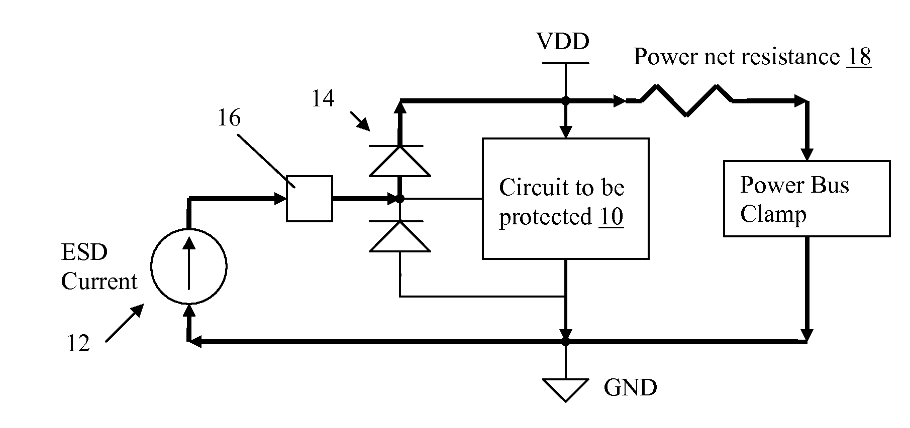
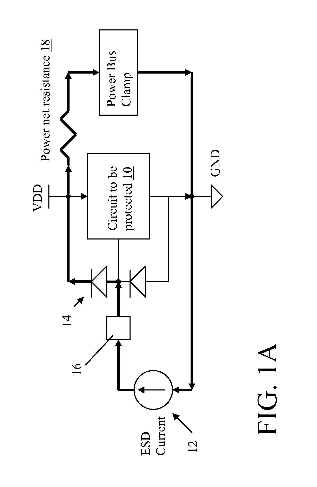
[0023]This disclosure provide two different approaches for providing active ESD protection, which include: (1) State Manipulation, in which the circuit to be protected is put into a predefined state during an ESD event to improve its ESD robustness; and (2) Current Injection, in which ESD current from the pad is intentionally injected into internal circuit nodes to raise their potential in order to achieve optimal voltage sharing across devices in the circuit. One or both could be utilized within an integrated circuit to provide ESD protection.

I. State Manipulation

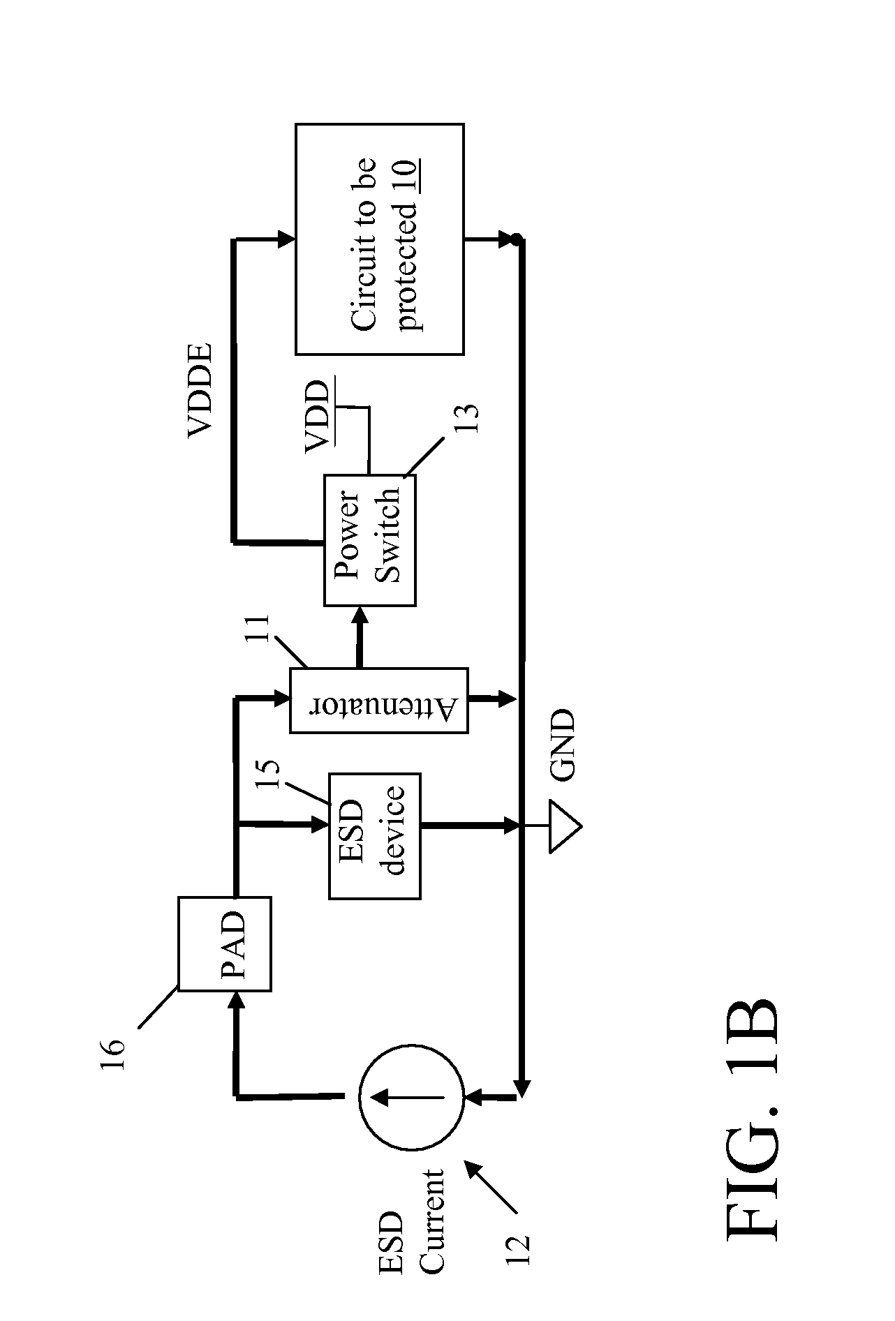
[0024]The use of state manipulation for providing ESD protection may be summarized as follows. First, a circuit is provided that is powered up by a portion of the ESD discharge current. Second, an ESD detector circuit is provided to detect an ESD event. Third, the circuit to be protected is placed into a predefined state by control circuits responding to the ESD detector. Fourth, the predefined state is implemented such th...


PUM


Abstract

A system and method of electrostatic discharge (ESD) protection in a logic circuit using either state manipulation or current injection. A first system is disclosed that includes an ESD detection circuit for detecting an ESD event; and an ESD control circuit that can change a state of the logic circuit from a normal mode to an ESD mode in response to a signal received from the ESD detection circuit. A second system is disclosed that includes an attenuator circuit coupled to a chip pad; and a switch for diverting current from the attenuator circuit to an internal node of the logic circuit during an ESD event to reduce a voltage at the chip pad.

Description

FIELD OF THE INVENTION[0001]The invention relates generally to providing electrostatic discharge (ESD) protection to integrated circuit devices, and more particularly relates to a system and method of providing active ESD protection using state manipulation and current injection.BACKGROUND OF THE INVENTION[0002]ESD, or electrostatic discharge refers to the usually sudden transfer of an ESD voltage potential from one object to another with a lower potential either by inductance or direct contact. ESD protection refers to a system of protecting an integrated circuit from ESD events.[0003]Standard ESD protection depends primarily on simple semiconductor devices (e.g., diodes or snapback n-type field effect transistors (NFETs)) to conduct ESD current safely to the power supply networks. The primary characteristic of a good ESD device is a low voltage drop in the conducting mode. If the ESD current produces a voltage on the chip pad that exceeds the breakdown voltage of circuits or devic...

Claims


Application Information

Patent Timeline
Patent Type & Authority Applications(United States)
IPC IPC(8): H02H9/00
CPCH01L27/0251
Inventor BRENNAN, CIARAN J.CHANG, SHUNHUA T.
Owner IBM CORP
Why Eureka
Try Eureka