Insulation Substrate, Power Module Substrate, Manufacturing Method Thereof, and Power Module Using the Same

Active Publication Date: 2007-12-27
MITSUBISHI MATERIALS CORP
View PDF2 Cites 12 Cited by
  • Summary
  • Abstract
  • Description
  • Claims
  • Application Information

AI Technical Summary

Benefits of technology

[0035] According to the above configurations, reduction of the line width, and a large current and a high voltage of the conductive pattern can be realized, and simultaneously joining strength of the conductive pattern and the surface of the ceramics substrate can be improved. In addition, since the substantially entire surface of the rising surface of the conductor is covered with the brazing filler metal, when the power module having the insulation substrate is used, it is possible to suppress occurrence of a situation that the power module is not appropriately used, for example, the rise of the rising surface becomes a singular point and a spark occurs in that portion as a start point or the conductor is electrically connected to an adjacent conductor.
[0036] According to the method of manufacturing a power module substrate of the invention, the conductive pattern can be provided on the surface of the ceramics substrate, without performing etching. Therefore, high-efficiency production of the power module substrate and reduction of the line width of the conductive pattern can be realized.
[0037] Further, according to the insulation substrate, the p

Problems solved by technology

However, as for the large conduction area, since there is a limitation on design of the apparatus itself in which the power module is incorporated, the external size of the ceramics substrate cannot be increased, and thus the width and thickness of the conductor cannot be increased.
For this reason, compactness as the latter requirement cannot be achieved.
Accordingly, there is a problem in that both requirements are not satisfied simultaneously.
The increase in the thickness of th

Method used


Image

  • Insulation Substrate, Power Module Substrate, Manufacturing Method Thereof, and Power Module Using the Same
  • Insulation Substrate, Power Module Substrate, Manufacturing Method Thereof, and Power Module Using the Same
  • Insulation Substrate, Power Module Substrate, Manufacturing Method Thereof, and Power Module Using the Same

Examples


Example

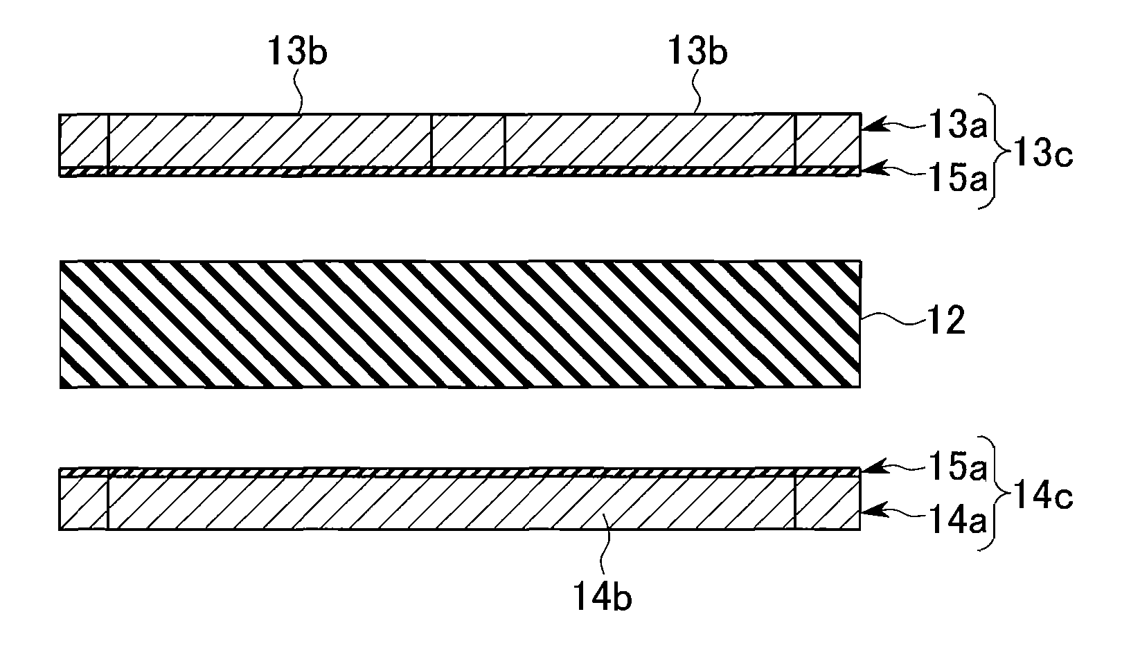
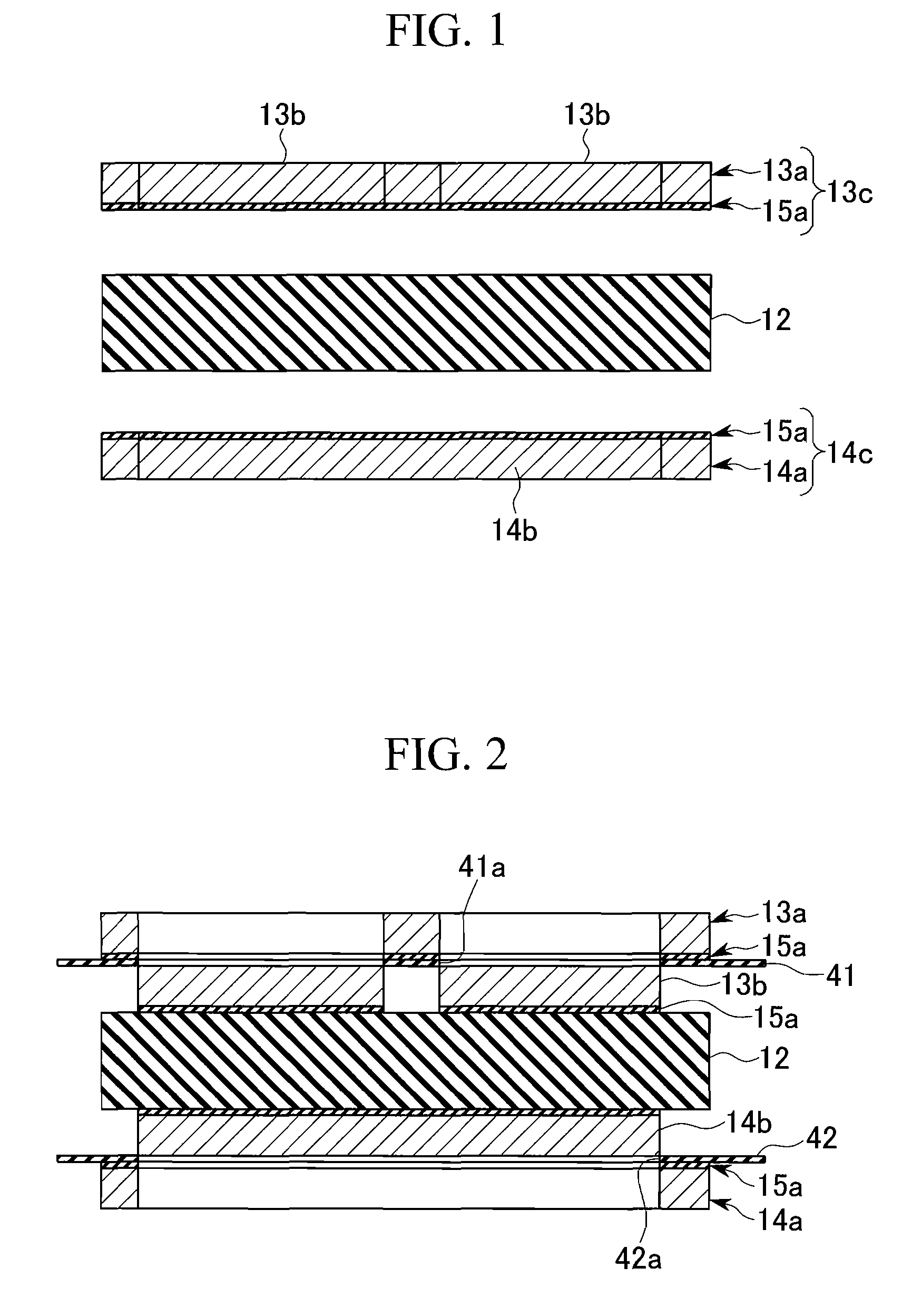
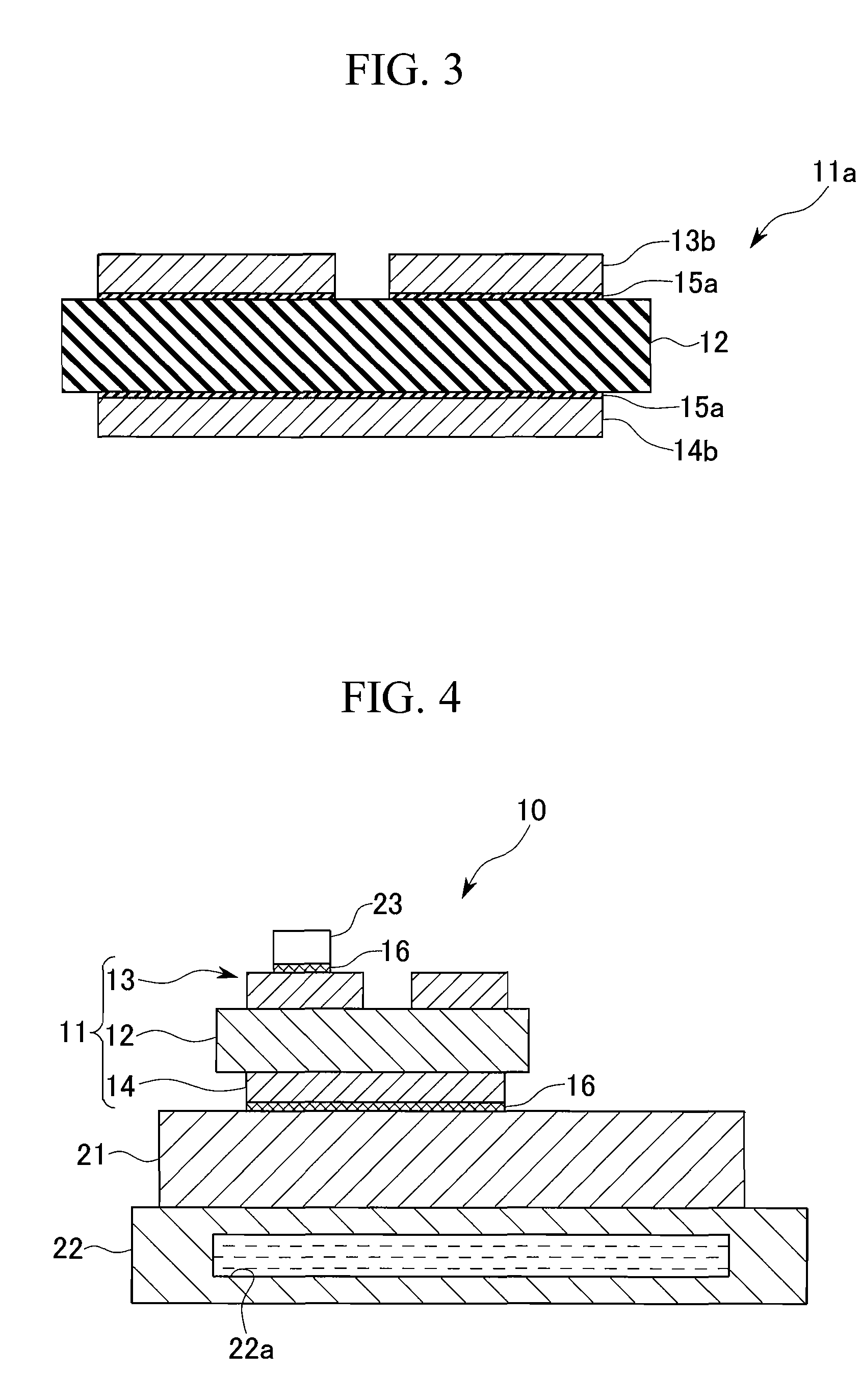
[0046] Hereinafter, an embodiment according to the first group will be described with reference to the drawing. FIGS. 1 to 3 are process views a method of manufacturing a power module substrate according to the first group. FIG. 4 shows a power module 10 to which a power module substrate formed by the manufacturing method shown in FIGS. 1 to 3. The power module 10 includes a power module substrate 11, a radiating element 21, a cool sink 22, and a semiconductor chip 23 serving as a heating element.

[0047] In the power module substrate 11, a conductive pattern 13 is provided at an upper surface of a ceramics substrate 12 formed of AlN, Al2O3, Si3N4, or SiC, and a metal layer 14 is provided at a lower surface thereof. The conductive pattern 13 and the metal layer 14 are formed of pure aluminum or an aluminum alloy, and are joined with the ceramics substrate 12 by an Al—Si or Al—Ge brazing sheet 15a, as described below.

[0048] Then, the semiconductor chip 23 is joined with an upper surf...


PUM

PropertyMeasurementUnit
Heightaaaaaaaaaa
Heightaaaaaaaaaa
Heightaaaaaaaaaa

Abstract

High-efficiency production of a power module substrate and reduction of the line width of a conductive pattern, and to provide an insulation substrate suitable for realizing a large current and a high voltage of a power module. A brazing sheet is temporarily fixed on a surface of a ceramics substrate by surface tension of a volatile organic medium, and a conductive pattern member punched from a base material is temporarily fixed on a surface of the brazing sheet by surface tension. These are heated so as to volatilize the volatile organic medium and a pressure is applied to the conductive pattern member in its thickness direction. The brazing sheet is melted to join the conductive pattern member with the surface of the ceramics substrate.

Description


Claims


Application Information

Patent Timeline
Owner MITSUBISHI MATERIALS CORP
Why Eureka
Try Eureka