

Semiconductor device and method for manufacturing same
- Summary
- Abstract
- Description
- Claims
- Application Information
AI Technical Summary
Benefits of technology
Problems solved by technology
Method used
Image

Examples
first example
[0054](First Example)
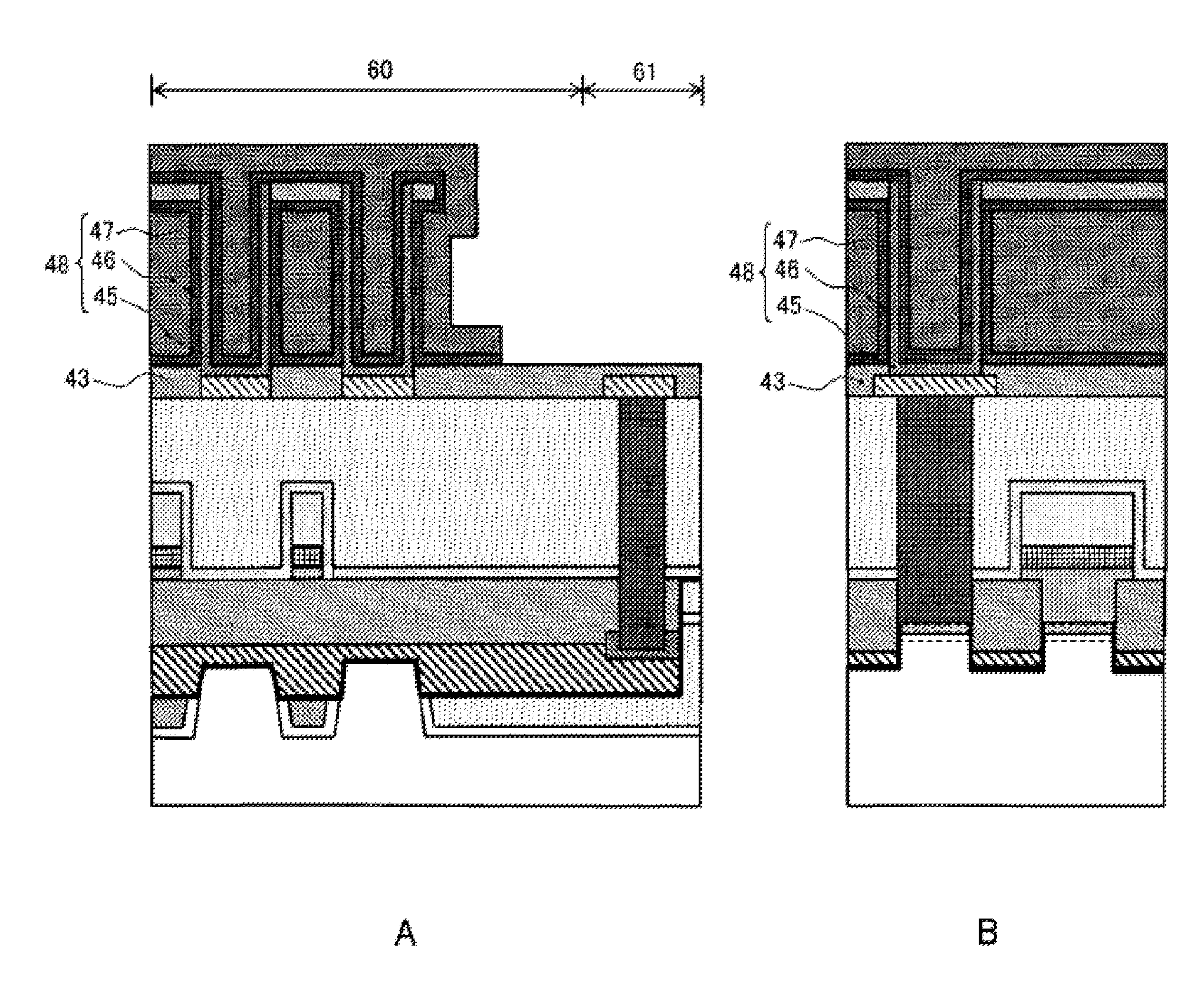
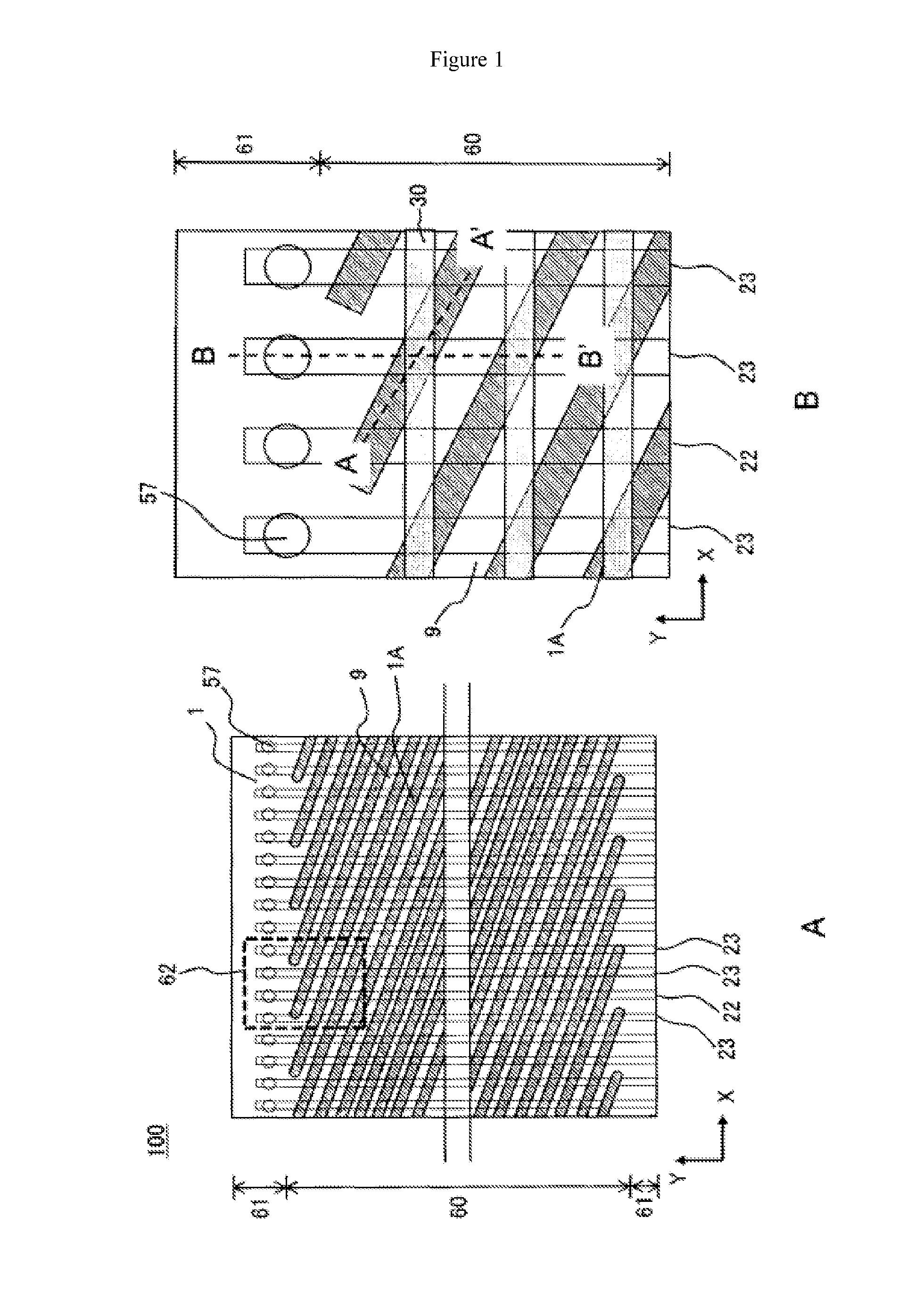
[0055]FIG. 1 is a plan view illustrating the configuration of a DRAM 100 according to this example, illustrating a memory cell region of the DRAM 100. FIG. 1A is a planar schematic diagram illustrating the arrangement of element isolation regions 9, active regions 1A, embedded gate electrodes 23 and embedded wiring lines for element isolation 22, in the DRAM 100, and FIG. 1B is an enlarged view of the part 62 enclosed by the dashed line in FIG. 1A. It should be noted that in FIG. 1 only the main structures are illustrated, in order to clarify the arrangement condition of the constituent elements.
[0056]As illustrated in FIG. 1, the DRAM 100 comprises a memory cell region 60 and peripheral regions 61 outside the memory cell region 60, in which drive transistors (which are not shown in the drawings) are disposed. The memory cell region 60 is provided with element isolation regions 9 (hereinafter referred to as ‘STIs (Shallow Trench Isolation) 9’) provided in a sili...
second example
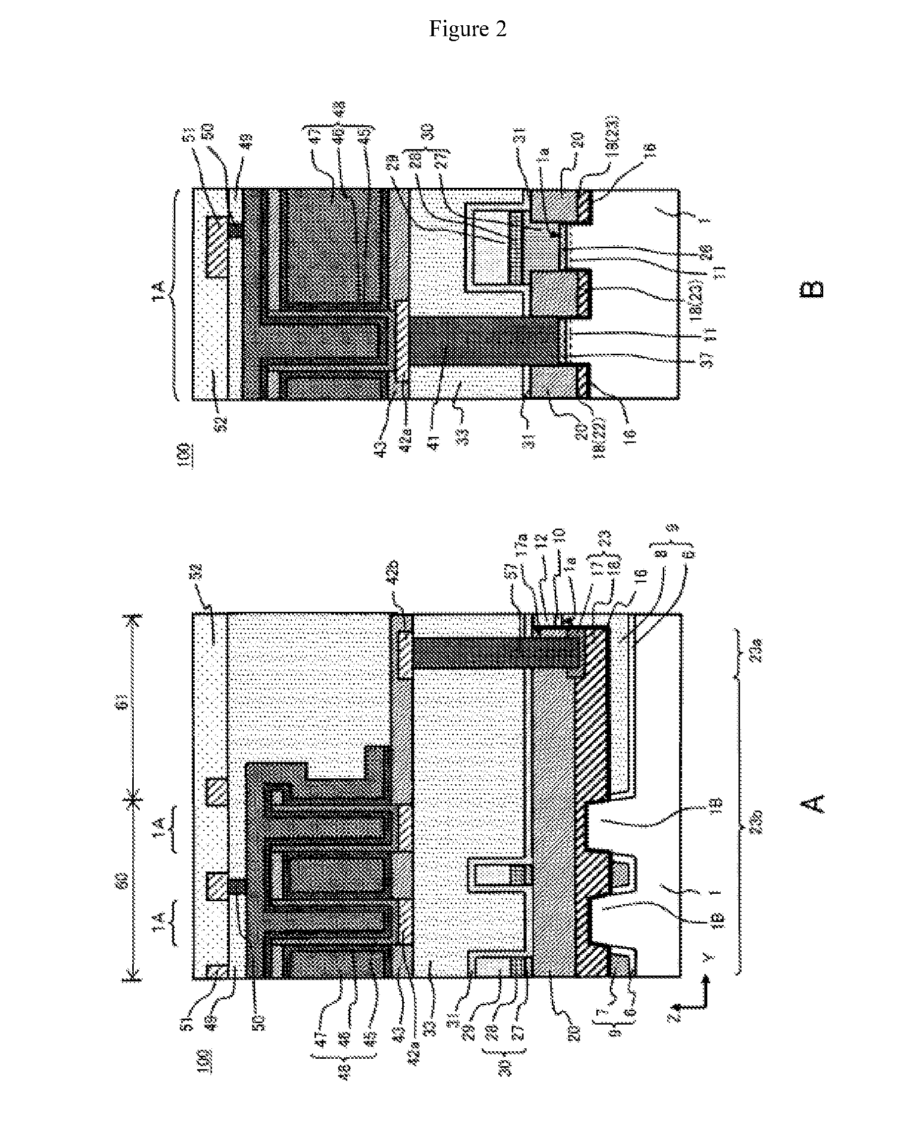
[0099](Second Example)
[0100]This example differs from the first example in that, in the embedded gate electrodes 23 and the embedded wiring lines 22, the width W1 of the part in contact with the contact plugs 57 (the first part provided with the titanium nitride film 18 and the tungsten film 17) is greater than the width W2 of the second part comprising the single-layer film of the titanium nitride film 18. Other structures in the semiconductor device in this example are the same as in the semiconductor device in the first example, and therefore the description here focuses on the structures that differ from the first example.
[0101]FIG. 25 is a plan view illustrating the semiconductor device in this example, illustrating only the embedded gate electrodes 23 and the embedded wiring lines 22, other structures being omitted. Further, the X-direction and the Y-direction in FIG. 25 represent the same directions as the X-direction and the Y-direction in FIG. 1 in the first example
[0102]As...
application examples
[0107](Other Application Examples)
[0108]In the abovementioned first and second examples, the semiconductor device and the method of manufacturing the same according to the present invention are described taking a DRAM as an example of a semiconductor device. However, the present invention can also be applied to other semiconductor devices provided with an electrode structure having a first part and a second part (for example PRAMs or ReRAMs).
[0109]Further, the single-layer film of the titanium nitride film' set forth in the scope of the patent claims indicates, for example, a single titanium nitride film having a uniform composition and formed using the same deposition method, laminated films comprising a plurality of titanium nitride films each having a mutually different nitrogen content, and laminated films comprising a plurality of titanium nitride films each formed using mutually different deposition methods.
[0110]Explanation of the Reference Numbers
[0111]1 Silicon substrate
[01...
PUM
 Abstract
Description
Claims
Application Information