

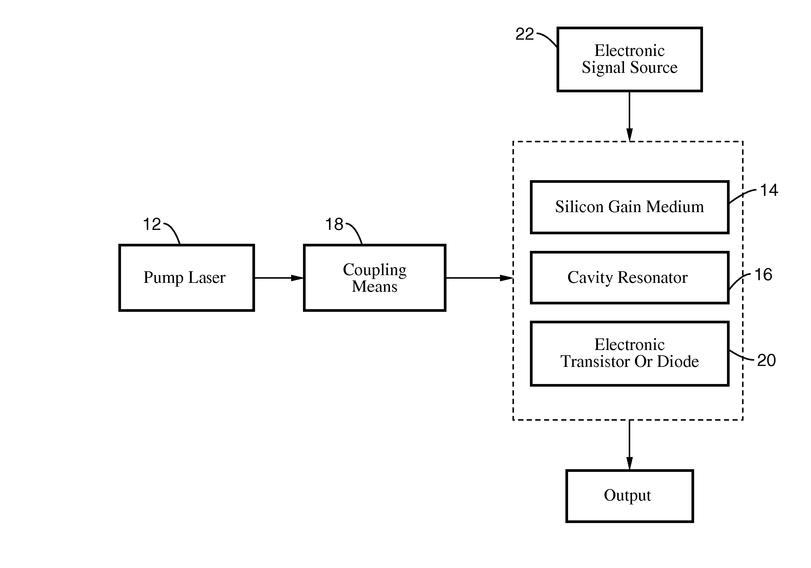
Cascaded cavity silicon raman laser with electrical modulation, switching, and active mode locking capability
a cascaded cavity, laser technology, applied in the direction of laser details, basic electric elements, electrical equipment, etc., can solve the problems of short pulse operation of such lasers, difficult to realize, and inability to fabricate transistors or diodes,
- Summary
- Abstract
- Description
- Claims
- Application Information
AI Technical Summary
Benefits of technology
Problems solved by technology
Method used
Image

Examples
example 1
[0055] A modelocked fiber laser 50 operating around 1540 nm with a 25 MHz repetition rate is used as a pulsed pump laser. In the present experiment, to prevent excessive spectral broadening and the pulse distortion in the amplifier and in the fiber patchcords, the pulses are broadened to 30 ps in a spool of fiber 52 before amplification using an erbium doped fiber amplifier (EDFA) 54 to the desired peak power. A tapered Silicon-On-Insulator (SOI) rib waveguide 56 approximately 2 cm in length and with a total insertion loss (coupling plus propagation) of 0.8 dB, is used as a gain medium. We first characterize the Raman gain in the silicon waveguide 56, using a CW laser at 1675 nm (Stokes wavelength) as the probe signal. Gain is measured by observing the enhancement of the probe signal in the presence of the pump pulse. The results, shown in FIG. 4, indicate that the silicon waveguide provides up to 9 dB of on-off gain at 25 W of peak pump power.
[0056] The setup f...
example 2
Stokes and Anti-Stokes Emission
[0060]FIG. 9 shows the block diagram of the silicon Raman laser as utilized. A modelocked fiber laser 50 operating at 1540 nm with 25 MHz repetition rate is used as a pulsed pump laser. After broadening the laser pulse width to 30 ps in a spool of standard Single Mode Fiber (SMF) 52 and amplification using an EDFA 54, the pump pulses are coupled into the laser cavity by a Wavelength Division Multiplexer (WDM) coupler 58. The output of the WDM is coupled to the silicon waveguide 56, which provides the optical gain. The waveguide 56 is approximately 2 cm long with measured 0.8 dB fiber-to-fiber insertion loss. At the waveguide output, a tap coupler 60 directs 95% of the power back to the input WDM coupler 58 to form a laser ring cavity. Two Polarization Controllers (PC) 62 are inserted, one on the pump arm and one in the cavity, to adjust the relative polarizations of the pump and the laser. The total length of the cavity is ˜8 m and adjusted to obtain ...
example 3
Direct Electrical Modulation
[0065] A laser was constructed using a silicon chip and a fiber loop cavity as illustrated in FIG. 13. The chip contains a waveguide 56 plus a p-n junction diode 80 (FIG. 14). The p-n junctions 82a, 82b are 8 μm away from the edge of the rib waveguide 56 and they do not induce additional propagation loss due to this large gap. The waveguide 56 is 2 cm long, has input and output tapers, and has a total insertion loss of 1 dB. The modal area is approximately 5 μm2. We used 30 ps pump pulses at 20 MHz repetition rate and at a wavelength of 1560 nm. These were generated by broadening 1 ps pulses generated by a Calmar Optocom modelocked fiber laser 50 in a piece of standard single mode fiber 52. The laser cavity is formed using a fiber ring configuration. Following the silicon waveguide 56, a tap coupler 60 with 5 to 95% splitting ratio is used to extract 5% of the power as the output. The 95% output of the tap coupler 60 is looped back into the WDM coupler 5...
PUM
 Abstract
Description
Claims
Application Information